Clear Sky Science · en
Advancing non-faradaic impedance biosensors: sensitivity enhancement strategies using microfluidics, multiscale labeling, and CMOS technology
Smarter Blood Tests on a Chip
Imagine a medical test that needs only a pinprick of blood, gives answers in minutes, and fits on a sliver of glass smaller than a postage stamp. This review article explores how a particular class of “electronic noses” for biology—called non-faradaic impedance biosensors—is rapidly approaching that vision. By cleverly combining tiny particles, microfluidic plumbing, and the same chip technology used in smartphones, researchers are boosting these sensors’ sensitivity by up to a million-fold, making it possible to spot disease markers at vanishingly low levels.
How These Tiny Electronic Noses Work
At the heart of these sensors are patterned metal fingers, known as interdigitated electrodes, printed on glass or silicon. When a liquid sample covers them, the electrodes feel how easily electrical charge builds up and rearranges at their surface. If target molecules—such as a protein linked to cancer or a bacterium in contaminated water—bind to a prepared surface between the electrodes, they slightly change this electrical behavior. Non-faradaic sensors focus on those subtle shifts in capacitance and resistance, without relying on chemical reactions or added dyes. This makes them simpler, more robust, and easier to shrink than many traditional electrochemical or optical tests. But because the raw signal from a few molecules is tiny, sensitivity has long been the main roadblock.
Building Better Sensor Surfaces
To make these chips selective, the metal and glass around the electrodes are coated with carefully chosen surface layers that act like molecular Velcro. On glass-like regions, silane molecules form ultra-thin films that expose chemical groups ready to grab antibodies, DNA strands, or other biological “hooks.” On gold electrodes, sulfur-bearing molecules snap into orderly monolayers that can be mixed to control spacing, resist nonspecific sticking, and keep the background signal stable. New electrode materials—such as graphene, laser-etched porous carbon, conductive polymers, and two-dimensional compounds called MXenes—dramatically increase the effective surface area and change how charge is stored at the interface. These advanced materials can strengthen the electrical response when a biomolecule binds, but they also risk adding extra noise and insulating layers, so surface chemistry must be tuned very carefully.
Amplifying Signals with Particles and Flow
One powerful strategy is to attach the target molecules to micro- or nanoparticles. Insulating beads, such as plastic or silica spheres, act like rocks in a stream: they block and redirect ionic currents near the electrodes, increasing resistance and lowering capacitance in a measurable way. Conductive particles, especially gold nanoparticles, do the opposite: they create new charge pathways and hot spots in the electric field, boosting capacitance and lowering resistance. Because a single bead is far larger than a protein, each binding event causes a much bigger electrical change—often improving detection limits by 10 to 15 times or more. Microfluidic channels add a second layer of amplification by pushing the sample across the sensor in a controlled way, speeding up how fast targets find their binding sites and washing away loosely attached contaminants. Clever designs using recirculating flow, capillary-driven channels, and finely tuned hydrodynamic forces can concentrate rare molecules and strip out background noise, cutting detection limits from the nanomolar range down toward picomolar and even attomolar levels.
Putting the Lab on a CMOS Chip
The third ingredient comes from mainstream electronics: complementary metal–oxide–semiconductor (CMOS) technology. By integrating dense arrays of interdigitated electrodes directly on CMOS chips, engineers place each sensing “pixel” only micrometers away from on-board signal generators and readout circuits. This shortens every electrical path, suppressing stray capacitances and external noise. Custom on-chip circuits generate clean sinusoidal test signals and then separate the real and imaginary parts of the sensor’s response, or directly extract magnitude and phase. Modern designs pack tens of thousands of pixels into a single device, making it possible to monitor single particles, individual cells, or many different biomarkers in parallel. Demonstrated systems already detect viral DNA at attomolar concentrations, cancer-related microRNAs at femtomolar levels, and even single bacteria on a pixel-by-pixel basis.
Where This Technology Is Headed
By combining particle labels, microfluidic control, and CMOS integration, researchers have shown that non-faradaic impedance sensors can rival or surpass more complex electrochemical approaches, achieving cumulative sensitivity gains greater than one million-fold. 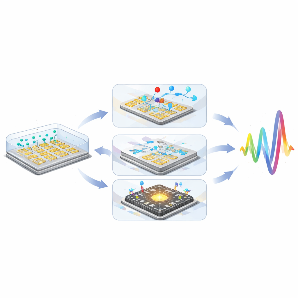
From Research Chips to Real-World Diagnostics
Looking ahead, the article envisions a new generation of “smart” biosensors that merge physical engineering with advanced algorithms and novel materials. Three-dimensional electrode structures and exotic 2D materials promise stronger electric-field coupling; microfluidic preconcentration and blood-plasma separation aim to clean and enrich samples on-chip; and machine-learning models trained on complex impedance spectra could automatically correct drifts and distinguish subtle disease patterns. 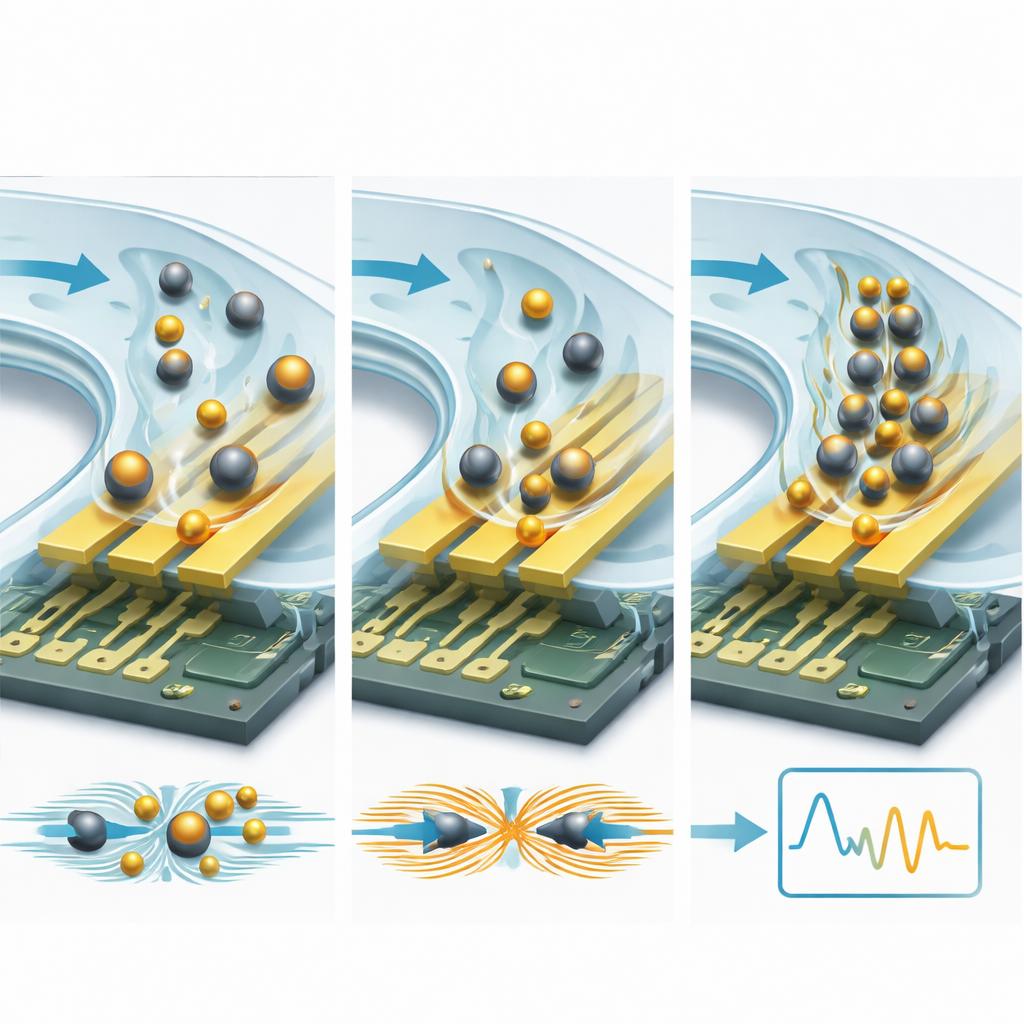
Citation: Kim, NS., Kim, J. Advancing non-faradaic impedance biosensors: sensitivity enhancement strategies using microfluidics, multiscale labeling, and CMOS technology. Microsyst Nanoeng 12, 117 (2026). https://doi.org/10.1038/s41378-026-01211-6
Keywords: impedance biosensors, microfluidics, nanoparticle labeling, CMOS biosensing, point-of-care diagnostics