Clear Sky Science · en
An energy-efficient Flash-SAR ADC with two-step flash structure in a 0.18 μm CMOS process
Why faster, thriftier chips matter
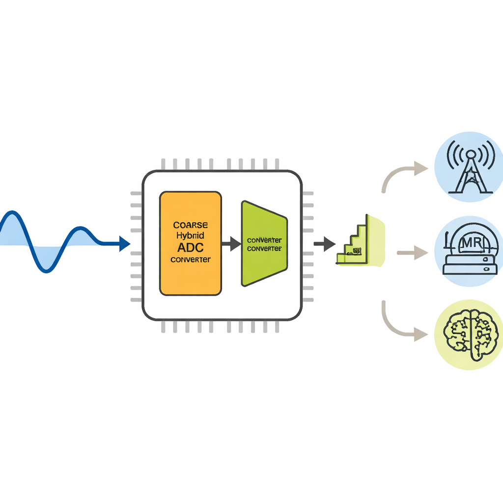
Every time your phone streams video, a smart sensor tracks your heartbeat, or an AI chip listens for a wake word, tiny circuits must translate real‑world signals—voltages and currents—into digital bits. These translators, called analog‑to‑digital converters, often set the limits on how quickly and efficiently devices can see and understand the world. This paper introduces a new converter design that aims to grab data very quickly while sipping power, a combination that could benefit many connected gadgets, medical tools, and AI systems.
Turning waves into numbers
At the heart of modern electronics lies a simple but demanding task: turning smooth analog waves into crisp strings of zeros and ones. Two classic approaches dominate. One, known for its blinding speed, compares the input signal against many fixed levels all at once, like dozens of judges raising scorecards in a single instant; this makes it fast but hungry for power and chip area. The other, more frugal approach works step by step, narrowing down the right value over several rounds; it uses far less hardware and energy but usually cannot keep up with very fast signals. Designing a converter that is both quick and efficient means blending the strengths of these two worlds.
A hybrid path that picks the best of both
The work described in this paper combines the two approaches into a single eight‑bit converter that runs at 100 million measurements per second in a mature chip process. The front of the circuit uses a small, fast stage to grab the rough value of the signal, while the back uses an energy‑saving step‑by‑step stage to refine the result. By splitting the job this way, the design avoids hundreds of always‑on comparison circuits while still reacting to incoming signals in a single instant. Careful timing control passes the rough result from the first stage to the second and orchestrates the sequence of comparisons without wasting clock cycles.
Smarter building blocks under the hood
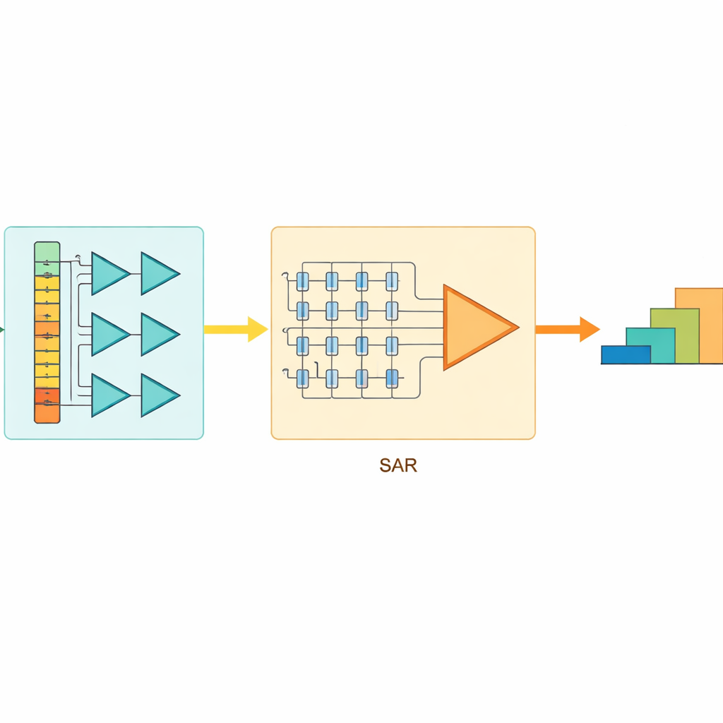
To make the fast front stage compact and efficient, the author uses a clever two‑step structure. Instead of comparing the input against sixteen levels at once, the circuit first decides which broad quarter of the range the signal lies in, then zooms in and compares within that smaller region. This trick cuts the number of comparison blocks from sixteen down to six. Those blocks themselves are built around a "floating" inverter amplifier that draws no steady current, pulling power only during brief moments of action. The design even lets two comparison steps share the same internal storage parts, trimming the silicon footprint further without slowing things down.
Fine tuning with gentle energy use
After the rough value is known, the second stage performs four quick refinement steps using an arrangement of capacitors that swings around a central voltage level. This style of switching reduces the energy lost every time the circuit charges and discharges, which is a major cost in many converters. A carefully crafted comparison block at this stage boosts small voltage differences in two steps, helping keep noise and unwanted kickback under control while still reacting rapidly. Simulations across different manufacturing conditions, temperatures, and supply voltages show that the circuit holds its accuracy well, even when disturbed by wide‑band electrical noise.
What the numbers say about real‑world impact
When tested in detailed computer models, the new converter reaches an effective precision close to its ideal eight bits while consuming just over four thousandths of a watt. Compared with earlier designs of similar size, it gains roughly one extra bit of useful precision over a traditional very‑fast converter and runs about 2,500 times faster than a purely step‑by‑step design in the same process, all while improving an overall efficiency score by nearly a factor of ten. In everyday terms, this means future radios, sensors, and AI accelerators built around this approach could capture richer signals at higher speeds without draining batteries as quickly, helping smart devices become both sharper and more sustainable.
Citation: Xue, S. An energy-efficient Flash-SAR ADC with two-step flash structure in a 0.18 μm CMOS process. Sci Rep 16, 13677 (2026). https://doi.org/10.1038/s41598-026-43435-6
Keywords: analog-to-digital converters, low-power electronics, mixed-signal circuits, internet of things, high-speed data acquisition