Clear Sky Science · en
3D atomic-scale metrology of strain relaxation and roughness in Gate-All-Around transistors via electron ptychography
Why Tiny Transistors Need a New Kind of Microscope
Every new generation of computer chips packs more power into less space, squeezing key components down to just a few billionths of a meter. At these scales, even a single misplaced atom or a slightly rough surface can slow a transistor or cause it to fail. Yet most tools that engineers use to look inside chips either cannot see individual atoms or cannot reveal what lies beneath the surface. This study introduces a powerful imaging approach that lets researchers map buried structures inside next-generation transistors in three dimensions, atom by atom.
From Flat Switches to Wraparound Wires
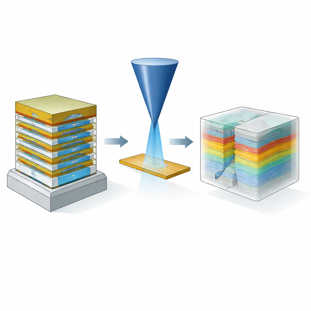
To keep improving speed and energy efficiency, chip makers have shifted from flat "planar" transistors to three-dimensional gate-all-around (GAA) designs. In GAA devices, the conducting channel is shaped as an ultra-thin silicon sheet, and the control gate wraps entirely around it through layers of insulating oxides and high‑k materials. This geometry offers superb control over the flow of electrons, which is crucial at extreme miniaturization. But it also creates buried interfaces and complex stacks of crystalline and glassy materials only a few atoms thick. These hidden boundaries can host roughness, voids, and other defects that strongly influence how well a transistor performs, yet they are very hard to measure directly in 3D with existing methods.
Limits of Today’s Imaging Tools
Traditional electron microscopes can form beautifully sharp pictures in two dimensions, but they struggle to tell what lies in front and what lies behind in thick samples. As electrons pass through many atomic layers, their paths bend and scatter in complicated ways, creating misleading contrast and blurring depth. Other tools, like X‑ray tomography or atom probe tomography, offer three‑dimensional views but either lack atomic resolution or have trouble with light elements and realistic device geometries. As gate lengths shrink below 10 nanometers, these shortcomings become critical: a single tiny void at the interface between silicon and its oxide, or a local patch of strain where atoms are pulled out of position, can drastically reduce electron mobility and shift a transistor’s operating voltage.
A New Way to See Inside: Electron Ptychography
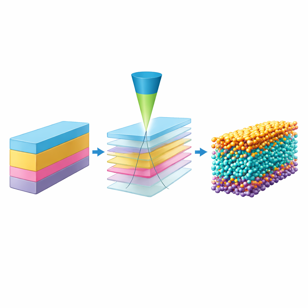
The authors demonstrate a computational imaging method called multislice electron ptychography that overcomes many of these obstacles. Instead of directly forming an image, the microscope scans a slightly defocused, overlapping probe across a thin cross section of the device while recording a full diffraction pattern at each position. These four‑dimensional data encode how the electron wavefront changes as it passes through the sample. Using advanced algorithms and a realistic model of how electrons propagate slice by slice, the method reconstructs the three‑dimensional electrostatic potential of the device at near‑atomic lateral resolution and nanometer‑scale depth resolution. Crucially, it faithfully captures both light atoms such as silicon and oxygen and heavier ones like hafnium, while correcting for multiple scattering that plagues conventional approaches.
Watching Interfaces, Roughness, and Strain in 3D
Applied to prototype GAA test structures, this technique reveals buried features that earlier methods either blurred or missed entirely. The reconstructions show stacking faults in the crystalline silicon channel, pinholes where hafnium oxide pushes into the channel, and step‑like edges at the silicon–oxide boundary. By tracking thousands of individual atoms through depth, the authors quantify how the silicon lattice gradually relaxes from a strained, distorted arrangement near the interface toward a more regular, bulk‑like structure in the center of a channel only about 5 nanometers thick. They find that roughly 40 percent of the silicon in these narrow channels remains in a strained state, a significant fraction for electron transport. They also directly measure how rough the buried interfaces are and how that roughness is correlated along the channel, uncovering clear differences between top and bottom surfaces that reflect each interface’s growth history.
What It Means for Faster and More Reliable Chips
Because the method delivers true three‑dimensional, atomic‑scale measurements of roughness and strain, it provides the real‑world input that device designers need for accurate simulations. Using simple models, the authors estimate that the rough and defect‑rich interfaces in these early GAA test devices could reduce electron mobility by factors of several to tens compared with a smoother reference interface. Just as important, the workflow—from preparing a sample to obtaining a 3D reconstruction—can fit into a few days and uses standard electron microscopes equipped with modern pixelated detectors. That makes it practical as a feedback tool during process development. In plain terms, this work shows that engineers can now "see" where their tiny transistors are going wrong, deep inside the device, early in the manufacturing flow. That visibility should help accelerate tuning of fabrication recipes, improve yields in advanced logic chips, and even guide the design of quantum devices that are highly sensitive to atomic‑scale disorder at buried interfaces.
Citation: Karapetyan, S., Zeltmann, S.E., Wilk, G. et al. 3D atomic-scale metrology of strain relaxation and roughness in Gate-All-Around transistors via electron ptychography. Nat Commun 17, 3561 (2026). https://doi.org/10.1038/s41467-026-69733-1
Keywords: gate-all-around transistors, electron ptychography, atomic-scale imaging, interface roughness, semiconductor metrology