Clear Sky Science · en
Power-efficient hardware architecture for 2-D multiple transforms in VVC
Why this matters for your screens
Streaming a 4K movie or holding a crisp video call may feel effortless, but under the hood it takes serious number-crunching and energy. As video moves toward 8K and beyond, today’s compression chips risk burning too much power, especially in TVs, game consoles, and mobile devices. This paper presents a new way to build the hardware at the heart of the latest Versatile Video Coding (VVC) standard, cutting power use while still handling ultra‑high‑definition video in real time.
From raw pixels to lean video
Every frame of a 4K video contains millions of pixels. If sent or stored directly, the data load would be enormous. Modern video standards like H.264, HEVC, and now VVC shrink this data by converting blocks of pixels into frequency patterns using mathematical operations called transforms. VVC gains extra compression by applying several transform flavors and block sizes, picking the best option for each patch of the image. This flexibility improves picture quality at lower bitrates, but it also makes the hardware more complex and power‑hungry.
The power problem inside video chips
Conventional hardware for VVC’s multi‑transform engine tends to keep large arrays of multipliers, adders, and memory blocks active even when only a small part is truly needed. Because 2‑D transforms are done as two 1‑D passes with an intermediate transpose step, existing designs often keep their transpose memories and coefficient stores switching for all block sizes, from tiny 4×4 up to 64×64. That constant activity wastes energy: unused memory banks still toggle, arithmetic units process idle data paths, and clock signals drive lanes that are not contributing to the current block. This undermines the efficiency gains promised by VVC, particularly in embedded and battery‑powered devices.
A smarter transform engine
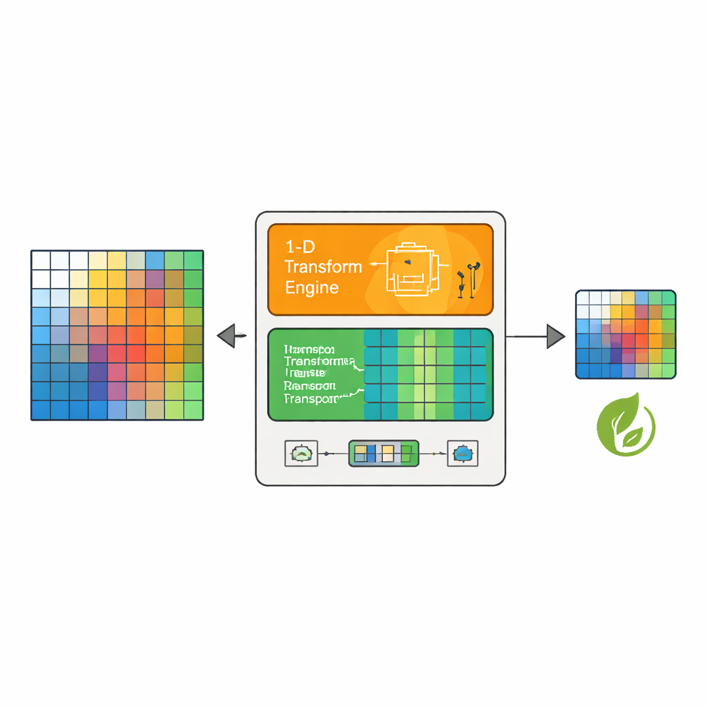
The authors propose a new 2‑D transform architecture that supports all square VVC block sizes and three key transform types (two cosine variants and one sine‑based type), while aggressively cutting dynamic power. At its core is a flexible 1‑D processing unit made of custom multipliers and adders built from basic logic rather than generic digital signal blocks. This choice allows the design to switch individual lanes on or off depending on block size. For a 4×4 block, only four multiplier lanes are active; for 8×8, eight lanes; for 16×16 and larger, more lanes are enabled in groups. This “selective gate isolation” reduces unnecessary switching inside the arithmetic tree, without sacrificing throughput, so that once the pipeline is full the hardware can produce one transformed value every clock cycle.
Reusing memory instead of duplicating it
Between the horizontal and vertical passes of the 2‑D transform, the intermediate data must be stored and then read out in rotated (transposed) order. Rather than using a single large, always‑on buffer, the design introduces a Unified Hybrid Transpose Memory (UHTM). This memory is divided into many small banks organized as tiles. Clever addressing logic ensures that writes arrive row by row and reads depart column by column, achieving the transpose purely by how locations are addressed rather than by moving data around. Only the banks that actually hold the current transform block are activated; all others remain idle. For small blocks such as 4×4 and 8×8, only one bank is used, while larger blocks progressively engage more banks, preserving energy for common small operations yet scaling cleanly to 64×64.
Proving it on real hardware
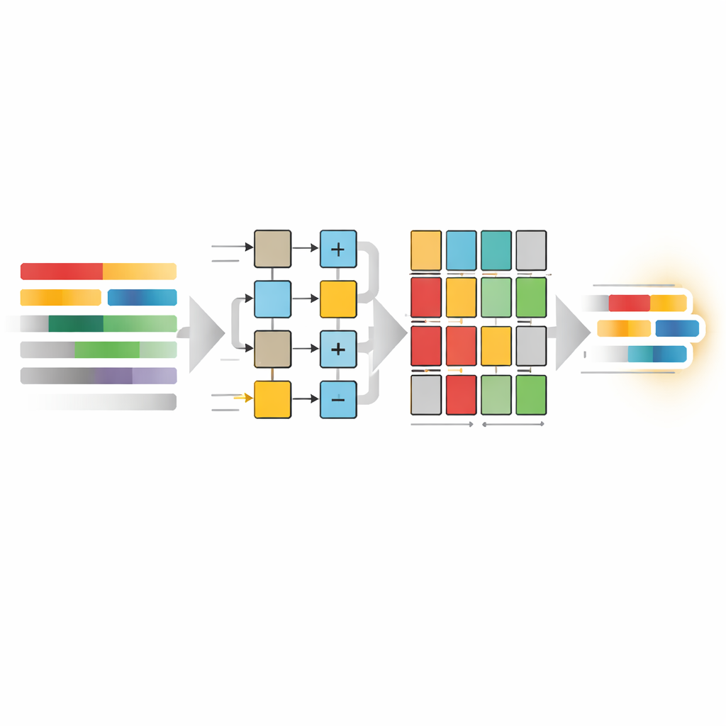
The team implemented their design on a Xilinx Zynq‑7000 field‑programmable chip and measured its behavior under realistic conditions. Running at nearly 349 MHz, the full 2‑D engine can handle ultra‑HD 4K video at 30 frames per second, outputting one transform coefficient per clock. Despite supporting more block sizes and transform types than many earlier designs, it consumes only 129 milliwatts of dynamic power, with an energy cost of about 370 picojoules per sample. Comparisons with other published hardware show that competing designs often use fewer logic cells but spend much more power, because they leave many arithmetic units and memory elements constantly switching. Here, fine‑grained clock gating, operand isolation, and bank‑aware memory control keep only essential circuitry active.
What this means for future devices
In plain terms, the authors demonstrate that smarter organization of work inside the chip—turning off what is not needed and reusing a single flexible core and memory—can deliver top‑tier video compression with far less wasted energy. Their architecture supports the full range of VVC transforms and sizes, operates at high speed, and is well suited to energy‑constrained systems like set‑top boxes, home gateways, and portable devices. With further refinements and custom chip fabrication, similar ideas could help tomorrow’s video hardware keep pace with rising resolutions and frame rates without overheating batteries or power bills.
Citation: Palagani, M.B., Nalluri, P. Power-efficient hardware architecture for 2-D multiple transforms in VVC. Sci Rep 16, 9908 (2026). https://doi.org/10.1038/s41598-026-40519-1
Keywords: video compression hardware, Versatile Video Coding, low power FPGA design, 2D transform architecture, 4K ultra HD processing