Clear Sky Science · en
System-conditioned reparameterization of the SCAN functional for accurate bandgaps: from analytical constraints to machine learning
Why tuning bandgaps matters
From smartphones and solar panels to LEDs and sensors, many modern technologies depend on semiconductors—materials whose ability to conduct electricity is set by a key quantity called the bandgap. This bandgap is notoriously hard to calculate accurately on a computer without using expensive methods. The paper explores a smarter, more flexible way to tweak an existing, widely used quantum‑mechanical recipe so it can predict bandgaps of many solids more reliably, without paying the heavy cost of the most advanced techniques.
A smarter dial on a trusted theory
The authors work within density functional theory, a standard approach for simulating materials at the atomic level. In this framework, the most delicate ingredient is the exchange–correlation "functional," a formula that encodes how electrons interact. A popular version called SCAN is built from rigorous physical constraints rather than heavy fitting to data, which makes it robust for many properties but only moderately accurate for bandgaps. Instead of inventing a brand‑new formula, the authors ask: what if we gently retune a handful of internal numerical knobs in SCAN on a material‑by‑material basis, so that it better reflects each solid’s bonding environment?
Tuning the recipe for different kinds of solids
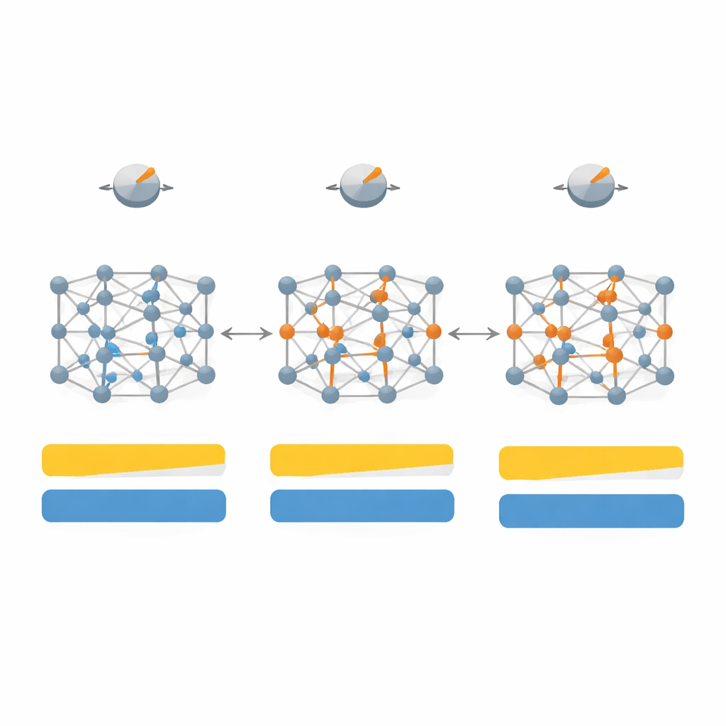
They first map out how changes in seven key parameters inside SCAN affect both the bandgap and the crystal structure for a set of 20 representative materials, including classic semiconductors like silicon and gallium arsenide, inert noble‑gas crystals, and strongly ionic salts such as lithium fluoride. By exploring this high‑dimensional parameter space, and then narrowing it to the four most influential knobs, they design a "system‑dependent" version of the functional they call SD‑SCAN. For covalent materials—where atoms share electrons in directional bonds—careful adjustments can push the calculated bandgaps close to experimental values while still keeping lattice constants, the basic dimensions of the crystal, essentially correct. In contrast, highly ionic materials, where electrons sit more rigidly on one kind of atom, remain difficult to fix with this approach, revealing a deeper limitation of the underlying formula.
How the electrons and light respond
Beyond just matching bandgap numbers, the team examines how their retuned functional changes the detailed electronic structure and how electrons are distributed between atoms. For covalent solids like diamond and silicon, SD‑SCAN shifts the empty energy bands upward and spreads charge more realistically along the bonds, strengthening their shared‑electron character. When they compute optical properties—how the material responds to light and high‑frequency electric fields—the improved bandgaps lead to more accurate dielectric constants and better agreement with measured spectra, especially for materials where the original SCAN either underestimated the gap or even mistakenly predicted metallic behavior.
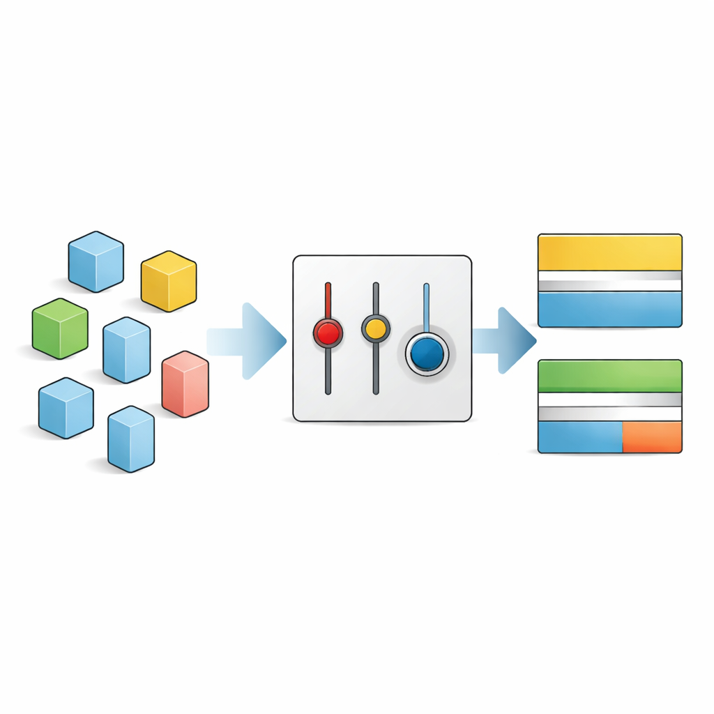
Letting data choose the right knobs
Manually tuning parameters for each new material would quickly become impractical, so the authors turn to machine learning to automate the process. They assemble a larger dataset of 260 semiconductors and insulators and, for each one, determine which parameter choices work best. Using simple descriptors—such as crystal symmetry, how strongly atoms share or transfer electrons, and how densely packed the atoms are—they train regression models to predict the optimal internal settings of SCAN from these physical features alone. Their best model, a multiple linear regression, can estimate bandgaps with significantly lower average error than standard SCAN, coming close to the ideal, fully hand‑tuned SD‑SCAN, yet at essentially the same low computational cost.
A shortcut for everyday calculations
As an even simpler alternative, the authors identify one crucial parameter that particularly affects semiconductors and insulators and propose a fixed re‑tuned version they call SCAN‑0.2. This variant keeps all of SCAN’s physics intact but slightly reshapes how it treats different bonding environments. Across their large test set, SCAN‑0.2 systematically improves bandgap predictions compared with the original functional while retaining very accurate crystal structures. It performs on par with the machine‑learning approach for many systems, offering a convenient drop‑in replacement for routine materials modeling.
What this means for future materials design
In plain terms, the study shows that a widely used theoretical tool for simulating materials can be made noticeably better at predicting bandgaps simply by learning how to set its internal dials based on the kind of solid being studied. For covalent semiconductors—the workhorses of electronics—the approach delivers gaps and optical responses close to experiment at a fraction of the cost of the most advanced methods. At the same time, the remaining difficulties with highly ionic compounds underline where new physics, not just better fitting, is needed. Together, the system‑dependent SD‑SCAN, the data‑driven ML‑SCAN, and the simple SCAN‑0.2 variant point toward a future in which exchange–correlation recipes are no longer one‑size‑fits‑all, but are adaptively tailored to each material, accelerating computer‑guided discovery of better electronic and photonic materials.
Citation: Dovale-Farelo, V., Tavadze, P., Marques, M.A.L. et al. System-conditioned reparameterization of the SCAN functional for accurate bandgaps: from analytical constraints to machine learning. npj Comput Mater 12, 162 (2026). https://doi.org/10.1038/s41524-026-02009-w
Keywords: semiconductor bandgaps, density functional theory, SCAN functional, machine learning in materials science, electronic structure