Clear Sky Science · en
A Rapid-prototyping CMOS-RRAM Integration Strategy
Why new memory on old chips matters
Our phones, laptops, and data centers all depend on tiny silicon chips that have followed Moore’s law for decades, cramming ever more transistors into the same area. That approach is now running into physical and economic limits. This article explores a different path: stacking a new kind of memory, called resistive memory, directly on top of familiar silicon electronics to create smarter and more efficient chips without shrinking features further.
Moving beyond just making transistors smaller
For years, progress in computing has meant making transistors smaller and packing more of them into a chip. Doing this today requires exotic tools and materials that are difficult and costly to use. The authors argue that, instead of only chasing smaller sizes, we can extend what existing chip factories already do well by adding new functions above the finished circuits. One promising option is resistive random access memory, a tiny device whose electrical resistance can be changed and remembered, so it can act both as storage and as a building block for brain inspired computing.
Designing a memory that can sit on top of silicon
To work in real products, this new memory must be made with the same kinds of materials and temperatures that conventional chip factories use. The team first developed and tested their resistive memory devices on standard silicon wafers, adjusting the materials until the cells switched at voltages that ordinary circuits can supply. By carefully choosing metal and oxide combinations and adding small amounts of nitrogen, they created memory cells that form and switch reliably at just a few volts, with smoothly adjustable resistance and good stability over time.
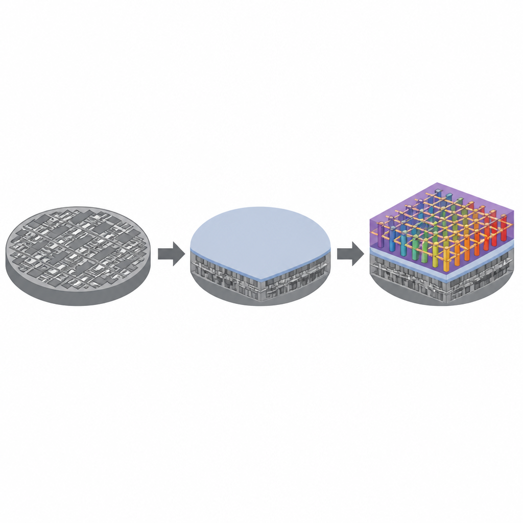
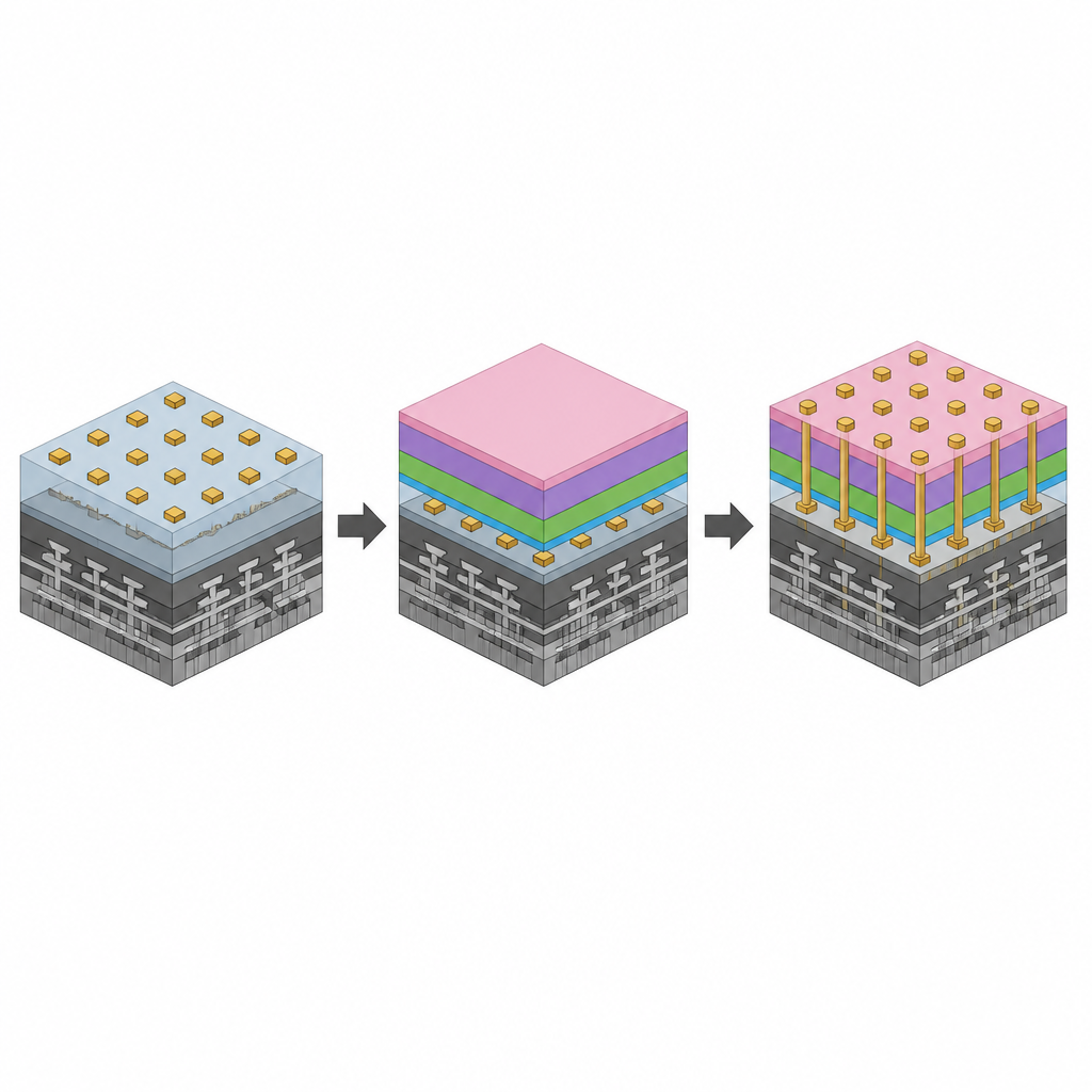
Building and checking the first integrated arrays
After tuning the basic devices, the researchers turned to the hard part: integrating thousands of them on top of ready made chips without damaging the underlying circuits. They thinned and smoothed the protective top layer of the foundry made wafers, then etched tiny openings down to buried metal lines. Into these openings they added the lower electrodes, the active resistive layer, and the upper electrodes, finally filling the etched holes with metal to connect everything together. Using this recipe, they built small test arrays where each memory cell is paired with a transistor, then showed that the original circuits still behaved as designed and that the new cells could be formed, programmed, and read reliably.
From tiny test blocks to dense and useful systems
With the basic process proven, the team scaled up to much larger and denser arrays containing up to a million potential memory cells. This required refining the surface smoothing and patterning steps so that very narrow lines could be drawn across the bumpy landscape of the finished chips. They mixed different lithography tools and tricks, such as double patterning, to reach smaller sizes while keeping development costs reasonable. Finally, they showed that the same integration method can support several kinds of real circuits, including neural signal interfaces, pattern matching units, neural network accelerators, and radiation tolerant memories, each using the resistive cells in ways tailored to the task.
What this means for the future of chips
Instead of waiting for ever smaller transistors, this work outlines a practical recipe for adding a new, flexible layer of memory directly on top of ordinary silicon chips. Because the approach uses standard materials and processes, it can bridge the gap between laboratory experiments and factory production. For a layperson, the takeaway is that future electronics may gain new abilities and efficiency not by shrinking further, but by smartly stacking new memory technologies on top of the chips we already know how to make.
Citation: Tsiamis, A., Stathopoulos, S. & Prodromakis, T. A Rapid-prototyping CMOS-RRAM Integration Strategy. Microsyst Nanoeng 12, 206 (2026). https://doi.org/10.1038/s41378-026-01335-9
Keywords: RRAM, CMOS integration, resistive memory, in memory computing, neuromorphic hardware