Clear Sky Science · en
High-efficiency grating couplers for vertical coupling in thin-film silicon nitride technology
Light Highways on a Chip
Our phones, data centers, and scientific instruments are increasingly turning to light instead of electricity to move information around. But to use light on a tiny chip, we need an efficient “on-ramp” that transfers light from a standard optical fiber into microscopic waveguides etched on a chip. This paper reports a new kind of on-ramp that works especially well for a promising material system called thin-film silicon nitride, pushing fiber‑to‑chip coupling losses closer to the levels needed for future ultra‑fast, low‑power photonic circuits.
Why Getting Light On and Off a Chip Is Hard
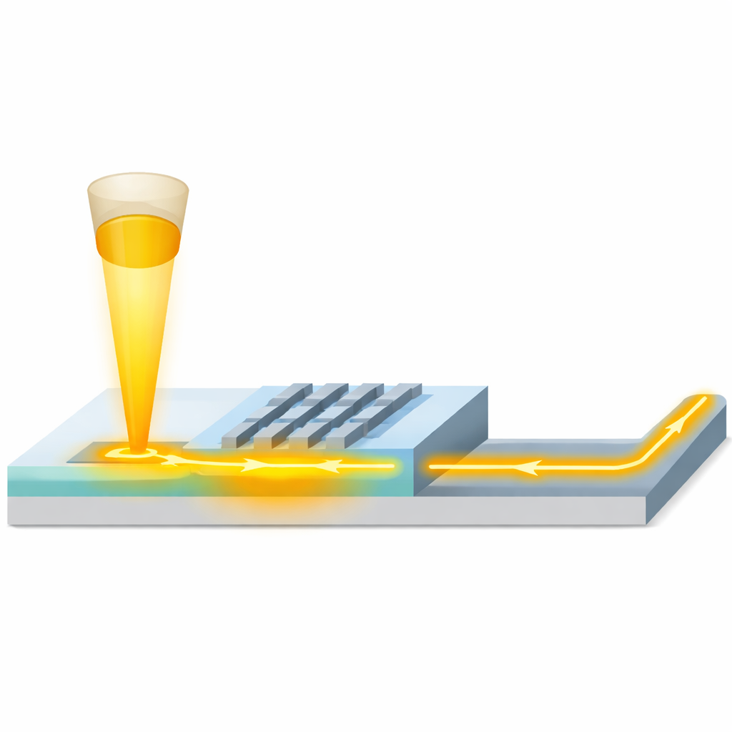
Photonic integrated circuits guide light through hair‑thin tracks on a chip to perform tasks such as sensing, communications, and even quantum experiments. While these waveguides can carry light with extremely low loss, connecting them to the outside world is surprisingly difficult. Standard optical fibers have a relatively large, soft light pattern, whereas chip waveguides confine light very tightly. If the shapes and directions of these light patterns do not match well, most of the light is reflected or lost, just like trying to push water from a wide hose into a narrow pipe with a poor fitting. Grating couplers—tiny periodic structures on the chip surface—act like finely tuned diffraction gratings that redirect light between the vertical fiber and the horizontal waveguide, but making them both efficient and easy to manufacture has been a major challenge.
The Promise and Problem of Thin-Film Silicon Nitride
Silicon nitride has become a star material in integrated photonics because it can guide light with extremely low loss over a wide range of wavelengths. In thin‑film versions, where the guiding layer is only tens to a couple of hundred nanometers thick, researchers have demonstrated waveguides with losses as low as a fraction of a decibel per meter—so low that light can circulate many millions of times in microscopic resonators. However, this thin geometry also makes the light only weakly confined to the core, which dramatically weakens the interaction between the guided light and any grating on the surface. As a result, standard grating couplers in thin‑film silicon nitride tend to be inefficient unless one adds extra layers like metal mirrors or high‑index overlays, which complicate fabrication and make devices sensitive to tiny process errors.
A New Two-Layer On-Ramp for Light
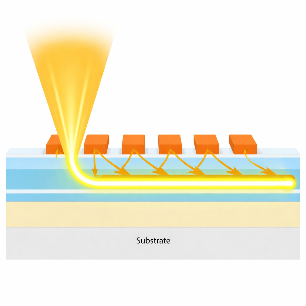
The authors solve this problem by stacking a carefully engineered layer of silicon-rich silicon nitride—essentially a denser, higher‑index version of the same material—on top of the thin silicon nitride waveguide, separated by a thin glass spacer. Only the top layer is patterned into a grating; the underlying waveguide remains intact, easing alignment demands between multiple etching steps. By gradually changing both the width of the grating teeth and the spacing between them along the length of the device, they tailor how strongly each section scatters light. This “apodization” and “chirping” strategy lets the grating extract or inject light in a controlled way so that the outgoing field profile closely matches the smooth, nearly Gaussian profile of a standard single‑mode fiber, while still directing most of the light upward toward the fiber rather than downward into the substrate.
From Computer Design to Real Devices
To find the best geometry, the team used detailed three‑dimensional simulations that track how light propagates through the layered structure. An automated optimization algorithm varied key parameters such as the thicknesses of the layers, the first grating period, and the rates at which the duty cycle and period change along the structure. The final design uses twenty grating periods and a relatively thick top silicon‑rich layer, which turns out to be more forgiving to fabrication errors than a thinner, silicon‑loaded alternative. Sensitivity studies showed that the new design maintains high performance even if the actual film thicknesses or grating dimensions deviate moderately from their ideal values, an important requirement for mass production with standard deep‑ultraviolet lithography tools.
Record Performance in a Straight-Down Configuration
After fabricating the devices on 200‑millimeter wafers, the researchers measured how much light was transferred from a vertically placed standard optical fiber into the on‑chip waveguide and back out through a second identical grating. By accounting for losses in the connecting waveguide, they extracted the efficiency of a single grating. At a wavelength near 1550 nanometers—the workhorse band for telecommunications—the new coupler achieves a record low loss of about 1.8 decibels per interface, and it maintains performance within 1 decibel over a bandwidth of roughly 31 nanometers. Notably, this is accomplished without any metal back‑reflector, index‑matching fluid, or tilted fiber; the fiber points straight down onto the chip, greatly simplifying packaging and wafer‑scale testing.
What This Means for Future Photonic Chips
For a non‑specialist, these numbers mean that far more of the light launched from a fiber actually makes it into the chip, and vice versa, than in previous thin‑film silicon nitride platforms. Better on‑ and off‑ramps reduce overall losses, relax power requirements, and simplify how photonic chips are tested and packaged in real products. Because the silicon‑rich nitride layer’s properties can be adjusted during deposition, the same design philosophy can be extended to different waveguide thicknesses and even other material systems. In essence, this work demonstrates a practical and fabrication‑friendly route to highly efficient fiber‑to‑chip interfaces, bringing low‑loss photonic circuits a step closer to widespread use in communications, sensing, and emerging quantum technologies.
Citation: di Croce, F., Vitali, V., Domínguez Bucio, T. et al. High-efficiency grating couplers for vertical coupling in thin-film silicon nitride technology. Sci Rep 16, 12880 (2026). https://doi.org/10.1038/s41598-026-44998-0
Keywords: integrated photonics, silicon nitride, grating coupler, fiber-to-chip coupling, photonic circuits