Clear Sky Science · en
Low-temperature wafer-scale growth of ultrathin tungsten disulfide for bifunctional interconnect barriers and liners
Why Shrinking Wires Need New Protection
Computers keep getting faster because engineers pack more tiny transistors and metal wires onto chips. As these copper wires shrink to just a few billionths of a meter wide, they run into new problems: the metal becomes less conductive and more fragile, and copper atoms can leak into surrounding materials, slowly killing the circuit. This article explores a new ultra‑thin coating—based on a material called tungsten disulfide—that could keep future chips running cooler, faster and longer.
A New Kind of Ultra-Thin Shield
Inside modern chips, the wiring network sits in what engineers call the “back end of line” layer, a stack of copper lines embedded in an insulating material like glass. Today each copper line must be wrapped in two separate coatings: a “liner” to help the metal stick and spread, and a “barrier” to stop copper atoms from wandering into the insulator. These traditional coatings are made of tantalum and tantalum nitride and together are several nanometres thick—so thick that in the tiniest future wires they would take up almost half the available space. The authors set out to replace this bulky double layer with a single, far thinner film that could do both jobs at once.
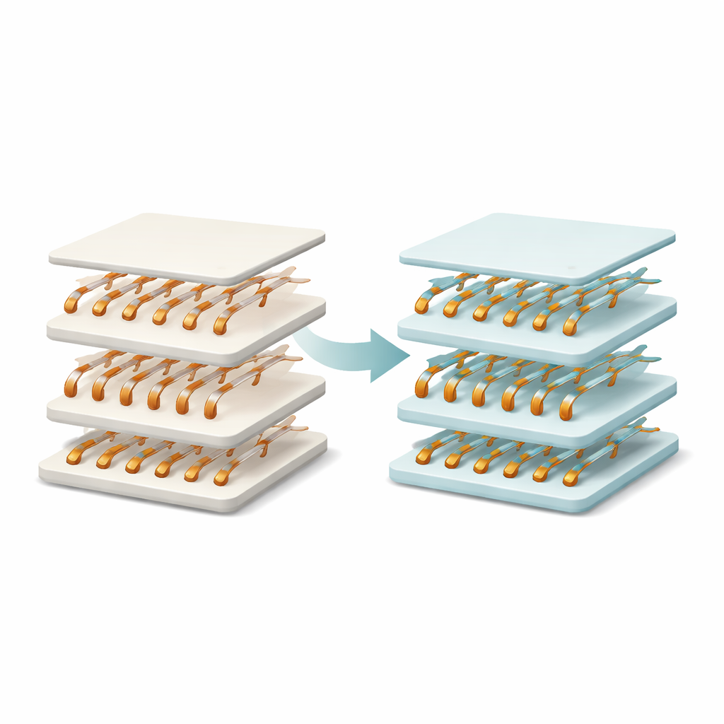
Growing a One-Atom-Thick Film Across a Whole Wafer
The team focused on tungsten disulfide (WS2), a so‑called two‑dimensional material that can be peeled down to a single sheet of atoms. They used a technique called atomic layer deposition to grow uniform WS2 films over standard 200‑millimetre silicon wafers at just 350 °C—cool enough not to damage finished chips. By adjusting the number of growth cycles, they could dial in the thickness precisely, from a single atomic layer (about 0.7 nanometres) to several layers and beyond. Electron microscopy images confirmed that the films covered even deep, narrow trenches—similar to the high‑aspect‑ratio features expected in advanced chip wiring—with more than 95% uniformity. In other words, the process can coat real three‑dimensional chip structures, not just flat test samples.
Helping Copper Spread Smoothly and Conduct Better
To test the WS2 layer as a liner, the researchers deposited very thin copper films—down to 10 nanometres—onto silicon dioxide with and without the WS2 coating. When they patterned these films into test wires and measured electrical resistance, the difference at small thickness was dramatic. Without the liner, 10‑nanometre copper behaved almost like an insulator; with a single WS2 layer underneath, the resistivity dropped by more than a million‑fold, and even beat state‑of‑the‑art tantalum/tantalum‑nitride stacks by about a factor of five. Microscopy revealed why: on bare glass the copper broke up into rough, disconnected islands, whereas on WS2 it formed a smoother, more continuous sheet with about half the surface roughness. That smoothness means electrons encounter fewer bumps and gaps, so the wire conducts far better even though the liner itself is much thinner.
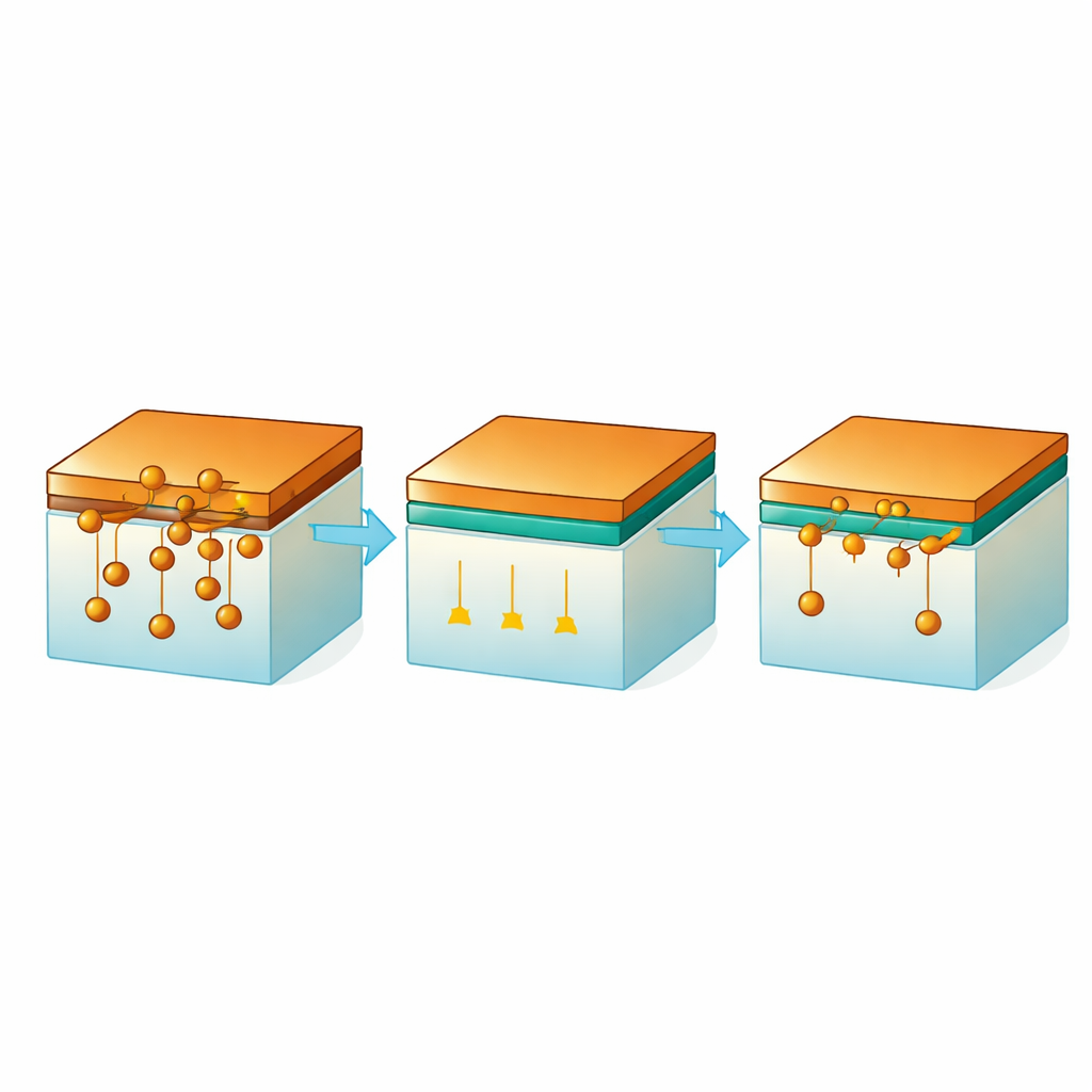
Blocking Copper from Leaking and Extending Lifetimes
The same ultra‑thin film also worked as a robust barrier. When copper was placed directly on silicon dioxide and heated to 400–500 °C, it reacted with the underlying material, forming large copper–silicon compounds and leaving behind a damaged, clumpy surface. With just one WS2 layer in between, the copper film stayed intact and the underlying silicon and oxygen remained clean, as confirmed by X‑ray and ion‑beam measurements. Under strong electric fields, devices containing the WS2 barrier survived roughly ten times longer on average before failing, compared with devices without any barrier. Thicker WS2 stacks performed even better, matching or surpassing conventional tantalum nitride despite being thinner.
How Atomic Structure Adds Extra Protection
To understand why these films block copper so effectively, the authors used computer simulations to model how individual copper atoms try to move through WS2. In a perfect sheet, copper faces a very high energy barrier to squeeze through. Real films, however, contain grain boundaries—tiny misfits between crystalline regions—that can open easier pathways. The calculations showed a key advantage of their growth method: in multilayer WS2, the grain patterns in different layers are not aligned. That misalignment forces copper atoms to navigate a zigzag path rather than a straight tunnel, raising the overall energy cost for diffusion. This atomic‑scale labyrinth helps explain why thicker WS2 stacks are especially good barriers.
What This Means for Future Chips
Taken together, the work demonstrates that a single, atomically thin WS2 film grown at chip‑friendly temperatures can both improve how copper wires conduct electricity and stop copper from leaking into surrounding materials. Because it is so thin and can coat complex three‑dimensional shapes across an entire wafer, this bifunctional layer could free up more space for copper in the smallest wires, keeping resistance and heat in check as chips continue to shrink. With further control over crystal grain structure and exploration of related two‑dimensional materials, this approach offers a promising route to more reliable, energy‑efficient electronics in the era beyond 5‑nanometre technology.
Citation: Mangattuchali, M.J., Astier, H.P., Chung, JY. et al. Low-temperature wafer-scale growth of ultrathin tungsten disulfide for bifunctional interconnect barriers and liners. Nat Electron 9, 379–388 (2026). https://doi.org/10.1038/s41928-026-01592-6
Keywords: tungsten disulfide, copper interconnects, 2D materials, atomic layer deposition, diffusion barrier