Clear Sky Science · en
Study on warpage stress in SiP packages during reflow soldering
Why tiny bends in electronics matter
Modern gadgets and AI hardware squeeze enormous computing power into packages smaller than a postage stamp. Inside these compact systems, chips, wiring layers and solder joints must survive extreme heating and cooling during manufacturing. Even slight bending—called warpage—can crack solder balls or break connections, quietly shortening a device’s life. This paper explores how and why these tiny structures bend during the soldering step, and how smarter computer models can help engineers design flatter, more reliable advanced chip packages.
How layered chip systems are built
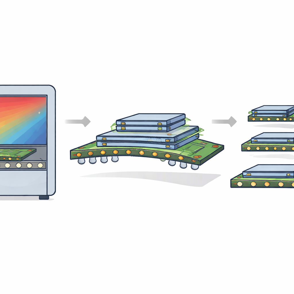
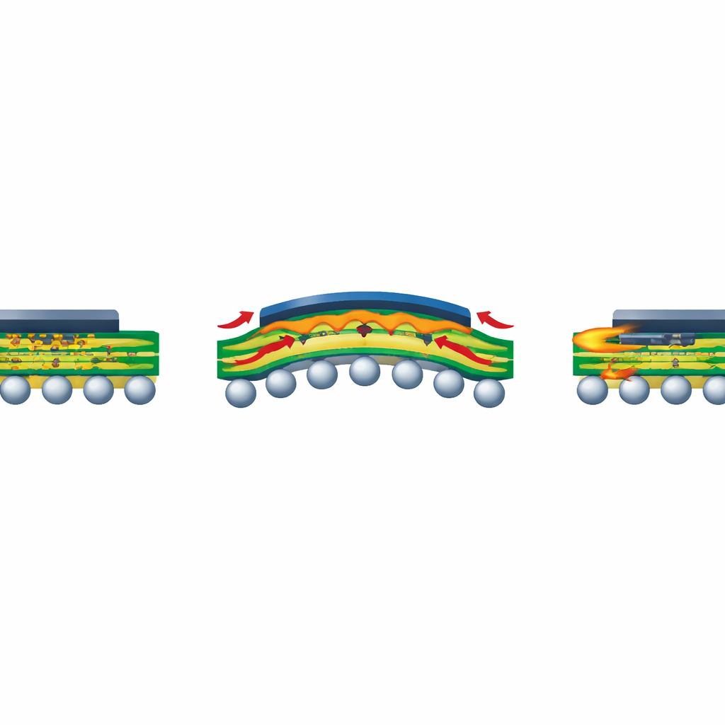
The study focuses on a type of advanced package called System‑in‑Package (SiP). Instead of a single chip on a simple board, a SiP stacks several chips on a high‑density circuit substrate made of many ultra‑thin layers. Copper lines route signals between chips, while small metal spheres (solder balls) connect the whole module to the main printed circuit board. During manufacturing, the assembly is passed through a reflow oven: its temperature rises from room temperature to around 240 °C and then cools again. Because copper, polymers and solder expand and contract by different amounts with temperature, the sandwich of materials can bow into a slight smile or frown shape, stressing everything inside.
Looking inside with realistic simulations
Earlier computer models of warpage often took shortcuts. They treated complex polymers as simple elastic solids, averaged out the fine copper wiring into uniform blocks, and ignored any bending that the board already had before soldering. This work builds a more faithful picture. The authors explicitly map the true copper trace patterns into the model and give key polymer layers "viscoelastic" behavior, meaning they can slowly relax under load like very stiff honey. They also include time‑dependent "creep" in solder balls, where metal slowly deforms under stress at high temperature. A carefully tuned mesh for the finite‑element model balances accuracy and computing time, and the overall method is checked against precise optical measurements of real boards, agreeing to within about 7 percent.
What really drives bending and stress
The improved simulations reveal several surprises. First, the bending pattern of the substrate flips between "smiling" and "frowning" shapes as temperature climbs above the softening point of the polymers and then drops again. Crucially, including the measured initial bend of the substrate changes peak warpage by tens of micrometers; ignoring it makes the assembly look safer than it truly is. The copper trace layout itself acts like hidden reinforcement bars: when modeled realistically with trace mapping, the predicted warpage shape becomes more wavy—matching experiments—rather than a simple bowl. The study also shows that just making the core board stiffer does not guarantee flatter packages. Because expansion is strongly direction‑dependent, a very stiff core can actually trap more stress, forcing the structure to bend more as a way to relieve that stress.
Choosing smarter materials, not just stronger ones
By swapping different dielectric and core materials in the model, the authors find that the "best" substrate is the one whose thermal expansion matches its neighbors and whose stiffness is moderate, not extreme. Among several candidate dielectric films, an engineering material labeled ABF‑L gives the lowest warpage because it expands less in the key temperature range of the reflow process. The study also compares traditional leaded solder with two lead‑free alloys. Classic Sn63Pb37 solder develops the lowest stress after soldering but the highest permanent deformation, making it more prone to fatigue cracks over many temperature cycles. One lead‑free alloy, SAC405, shows higher stress but much lower accumulated strain, which translates into better long‑term reliability for the tiny solder balls that hold the package up.
What this means for future electronics
In plain terms, the work shows that warpage in advanced chip packages is not controlled by any single "stronger is better" material choice. Instead, it emerges from how many layers with different thermal behaviors are stacked, how thin copper lines are arranged, and how metals and polymers slowly relax under heat. By capturing these effects in detail, the proposed simulation method predicts bending and stress much more accurately without demanding unmanageable computing resources. That gives designers a practical tool to choose substrate stacks and solder alloys that keep devices flatter and connections healthier, paving the way for more reliable, tightly packed electronics and AI hardware.
Citation: Qu, R.N., Li, D.S., Pan, L. et al. Study on warpage stress in SiP packages during reflow soldering. Sci Rep 16, 14326 (2026). https://doi.org/10.1038/s41598-026-38115-4
Keywords: electronic packaging, warpage, system-in-package, reflow soldering, solder fatigue