Clear Sky Science · en
Unsupervised defect clustering in atomic-resolution microscopy using a convolutional variational autoencoder
Why tiny flaws in crystals matter
Modern electronics, solar cells, and sensors all depend on materials that look perfectly ordered at the atomic scale. In reality, every crystal is sprinkled with tiny flaws—missing atoms, extra atoms, or slight shifts in the pattern—that can make a device more efficient or quietly kill its performance. The paper behind this summary presents a way to let artificial intelligence hunt for these flaws automatically in high‑resolution microscope images, without human labeling or expert tuning, opening a path toward faster and less biased materials discovery.
Letting a computer learn what “perfect” looks like
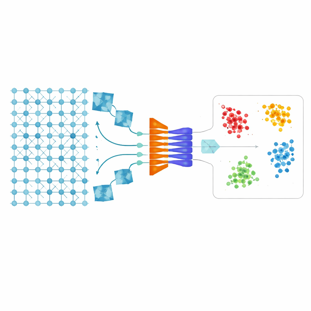
The researchers start from a simple idea: instead of teaching a computer every possible kind of defect, teach it only what a perfect crystal looks like. They use atomic‑resolution images from a powerful electron microscope, where each bright dot corresponds to a column of atoms. A special type of neural network, called a convolutional variational autoencoder, is trained on regions of the image that are believed to be defect‑free. Over time, this network learns the regular, repeating pattern of the crystal and becomes very good at reconstructing what an ideal, undisturbed lattice should look like.
Turning differences into a map of flaws
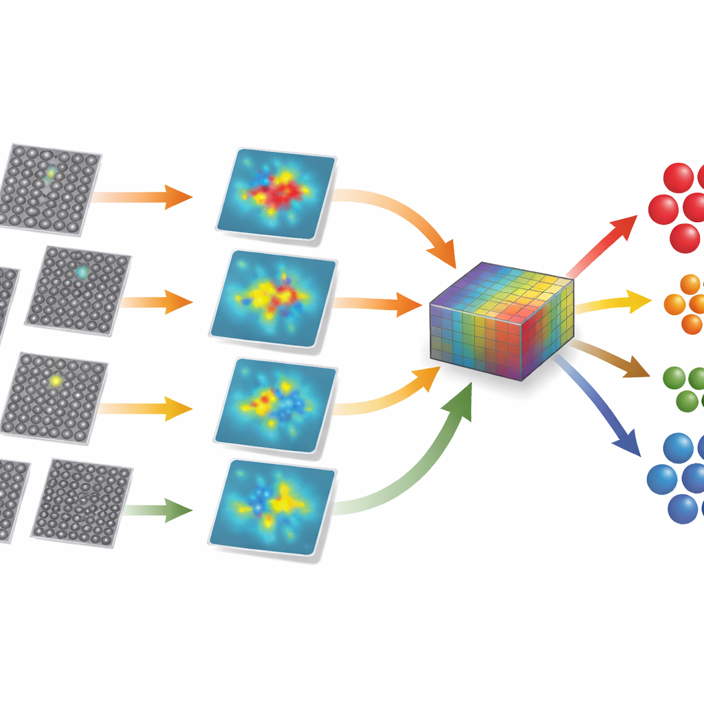
Once the network has learned the ideal pattern, each new microscope patch is fed through it. The model produces its best guess of a flawless version of that patch. By subtracting this guess from the real image, the method creates a “difference” picture that highlights only what does not fit the learned pattern—such as an extra atom, a missing dumbbell of atoms, or a shift in stacking. A further filtering step removes random noise and edge artifacts, leaving behind a clean signal that focuses on genuine structural oddities rather than on how the image window was cut. In effect, the system rephrases the problem from “learn all possible defects” to “find anything that is not normal.”
From raw images to meaningful groups
To sort these flaws into useful categories, the team converts each patch into a set of 47 simple numerical descriptors. These describe how bright the patch is on average, how lopsided its intensity distribution is, how many sharp features it contains, and how its patterns repeat in space, among other traits. They then prune this list in three stages: removing redundant descriptors that behave almost identically, discarding those that fail to separate images into distinct groups, and filtering out those that hardly vary at all. This shortlisting leaves a leaner, more informative collection of features that better captures real structural differences while cutting down on noise and computation.
Letting the data decide how many defect types exist
With these refined features in hand, the authors use standard clustering tools to let the data organize itself. They first compress the feature space using principal component analysis, which keeps the most important variations while shrinking the number of dimensions. Then they apply a classic clustering method, k‑means, many times while systematically varying both the number of clusters and the number of principal components. A quality measure called the silhouette score indicates how well separated the resulting groups are. By scanning across possibilities, the framework automatically identifies not only where the clusters lie but also how many defect types best describe the dataset—without any prior labels or manual choices.
Proving the approach on two different crystals
The method is tested on images of two well‑studied materials: cadmium telluride, used in thin‑film solar cells, and strontium titanate, a model oxide crystal. In cadmium telluride, the dataset includes bulk regions, several kinds of stacking faults, special dislocation structures, and twin boundaries, along with artificially added extra and missing atoms. Despite subtle differences in contrast and distracting edge effects, the framework automatically recovers seven distinct clusters that match these categories, with only a handful of misclassifications out of more than a thousand images. Applied to strontium titanate, where some defects differ only slightly from the perfect lattice, the same workflow again finds the correct number of groups and sorts images with high accuracy, showing that the approach is not narrowly tuned to one material.
What this means for future materials research
In plain terms, the study shows that a computer can teach itself to spot and group atomic‑scale defects in microscope images with minimal human guidance. By learning the normal pattern of a crystal and focusing on the differences, the system can sift through large image collections, discover distinct types of flaws, and do so on ordinary lab computers. This kind of unsupervised, automatic sorting could help researchers rapidly map how defects are distributed in a sample and how they relate to performance, laying the groundwork for more autonomous, data‑driven design and optimization of next‑generation materials.
Citation: Ayyubi, R.A.W., Sultanov, S., Buban, J.P. et al. Unsupervised defect clustering in atomic-resolution microscopy using a convolutional variational autoencoder. npj Comput Mater 12, 166 (2026). https://doi.org/10.1038/s41524-026-02024-x
Keywords: atomic defects, electron microscopy, unsupervised learning, autoencoders, materials characterization