Clear Sky Science · en
Ballistic transport in nanodevices based on single-crystalline Cu thin films
Electrons on a Superhighway
Modern electronics depend on steering floods of electrons through ever narrower metal wires. As chips shrink, those electrons bump into more obstacles, turning precious electrical energy into heat and limiting performance. This study reveals a way to build copper wires so clean and orderly that electrons can shoot through them almost as if on a frictionless superhighway, paving the way for cooler, faster, and more reliable devices.
Why Straight-Line Travel Matters
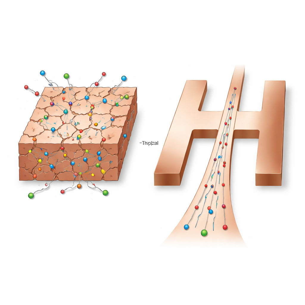
Inside ordinary metals, electrons usually move in a zigzag, constantly bouncing off impurities, crystal defects, and the boundaries between differently oriented grains of the material. When the distance an electron can travel without a collision is shorter than the size of the device, its motion is said to be diffusive, much like a crowd jostling its way through a busy marketplace. In the opposite case, when that distance exceeds the device size, electrons enter the ballistic regime. There, they preserve delicate quantum properties such as momentum, spin, and phase, which are key ingredients for next-generation quantum and low-power electronics.
Building Nearly Perfect Copper Films
Copper is already the workhorse metal for wires and connections in integrated circuits, but standard copper films are polycrystalline: they are made of countless tiny grains stitched together by grain boundaries. These internal seams act as roadblocks that scatter electrons and limit how far they can travel. The researchers used a refined sputtering method called atomic sputtering epitaxy to grow copper films that are single-crystalline along a favored orientation, known as Cu(111). In these films, the atoms line up in a continuous, highly ordered lattice across large areas, eliminating grain boundaries while leaving behind only twin boundaries, which disturb electrons far less.
Watching Electrons Take the Shortest Path
To test how electrons move in these ultra-clean films, the team carved them into narrow cross-shaped channels, with widths down to 150 nanometers and thickness around 90 nanometers. By driving current through one arm of the cross and measuring voltage on a neighboring arm, they monitored a quantity called bend resistance. In the usual diffusive case, this resistance is positive and changes with temperature in a way that matches well-known theories of how electrons scatter from vibrating atoms. For wider devices, their data followed this textbook behavior. But in the narrowest channels, the bend resistance dipped below zero at temperatures below about 85 kelvin, a counterintuitive signal that electrons were traveling ballistically, flying directly from the current source into the opposite arm instead of spreading out evenly.
Untangling the Role of Hidden Defects
The team then asked which microscopic features of the copper most strongly determine whether electrons can move ballistically. Using electron backscatter diffraction mapping and electron microscopy, they compared three types of films: conventional polycrystalline copper, copper with a reduced number of grain boundaries, and truly single-crystalline copper containing only twin boundaries. They found that resistivity—how strongly the film resists electrical flow—increased systematically with the total length of grain boundaries. In contrast, twin boundaries barely affected resistivity because they do not trap charge or strongly disturb the electronic structure. In the narrowest channels, once grain boundaries were removed, electrons could travel distances longer than the device width, allowing ballistic transport and negative bend resistance to appear.
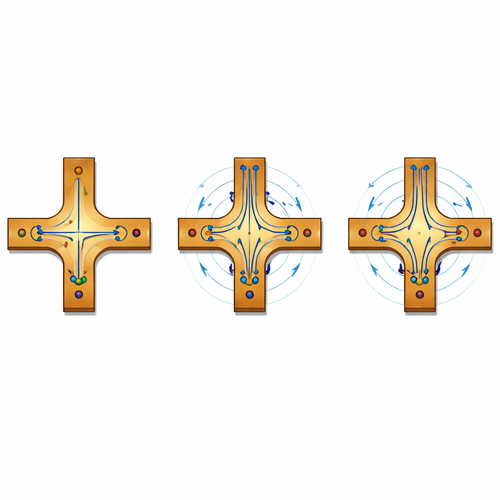
Magnetic Bends and Changing Charge Carriers
Applying a magnetic field perpendicular to the film added another twist. In ballistic devices, this field gently curves the straight-line paths of electrons, reducing how many reach the opposite contact and thus driving the bend resistance back toward positive values. The measurements matched expectations from quantum transport theory, reinforcing the ballistic picture. Hall-effect measurements, which reveal the types of charge carriers, showed that wider single-crystal films behave as if both electrons and holes carry current. As the channels shrink toward one-dimensional wires, calculations and experiments together indicate that the contribution from holes fades, leaving electrons as the dominant carriers, a direct consequence of quantum confinement in the tiny geometry.
What This Means for Future Devices
By demonstrating ballistic transport in scalable, deposited copper films, this work turns a familiar industrial metal into a promising playground for quantum and ultra-efficient electronics. Single-crystal Cu(111) nanodevices can preserve the quantum information carried by electrons over surprisingly long distances, which could help tackle long-standing issues like overheating and material fatigue in densely packed chips. Beyond immediate engineering benefits, these structures also provide a clean platform to explore the subtle topology of copper’s electronic landscape and other quantum effects that only become visible when electrons are free to travel without interruption.
Citation: Cho, Y., Kim, S.J., Jung, MH. et al. Ballistic transport in nanodevices based on single-crystalline Cu thin films. Nat Commun 17, 3602 (2026). https://doi.org/10.1038/s41467-026-70252-2
Keywords: ballistic transport, single-crystal copper, nanodevices, quantum electronics, grain boundaries