Clear Sky Science · en
Intermediates of forming transition metal dichalcogenide heterostructures revealed by machine learning simulations
Why stacking ultrathin materials is so hard
Electronics built from sheets just a few atoms thick promise faster, more efficient devices. A popular family of these ultrathin semiconductors is made from metals bound to sulfur or selenium, and when different sheets are stacked, they can behave like entirely new materials. But growing large, flawless stacks in the lab has proved tricky: the layers tend to mix into alloys instead of staying cleanly separated. This study uses advanced computer simulations powered by machine learning to peer into the hidden steps of how such stacks grow, revealing an unexpected intermediate structure that helps explain both the problems and new opportunities for devices.
Building atom-thin stacks for future chips
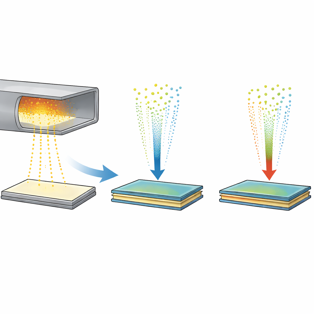
Engineers are especially interested in stacking materials such as molybdenum disulfide (MoS2) and tungsten disulfide (WS2). These so‑called van der Waals heterostructures conduct electricity well, interact strongly with light, and can be assembled like Lego bricks at the atomic scale. Mechanical stacking can produce beautiful, sharp interfaces, but only on tiny flakes and at high cost. Scalable methods like chemical vapor deposition can grow single layers across a whole wafer, yet when researchers try to stack different layers, the metals tend to swap places and form mixed alloys, spoiling the clean electronic behavior the devices need.
Using smart simulations as an atomic camera
Watching atoms move during growth in a real furnace is nearly impossible, so the authors built a highly accurate digital model instead. They trained a machine learning potential—an artificial intelligence model tuned on thousands of quantum‑mechanical calculations—to mimic how molybdenum, tungsten and sulfur atoms interact. Plugged into molecular dynamics simulations, this model let them track millions of atomic motions over nanoseconds while keeping near‑quantum accuracy. They verified that the model faithfully reproduced known structures, energies and vibrations, ensuring that its predictions for growth pathways are trustworthy.
A hidden metal layer that changes everything
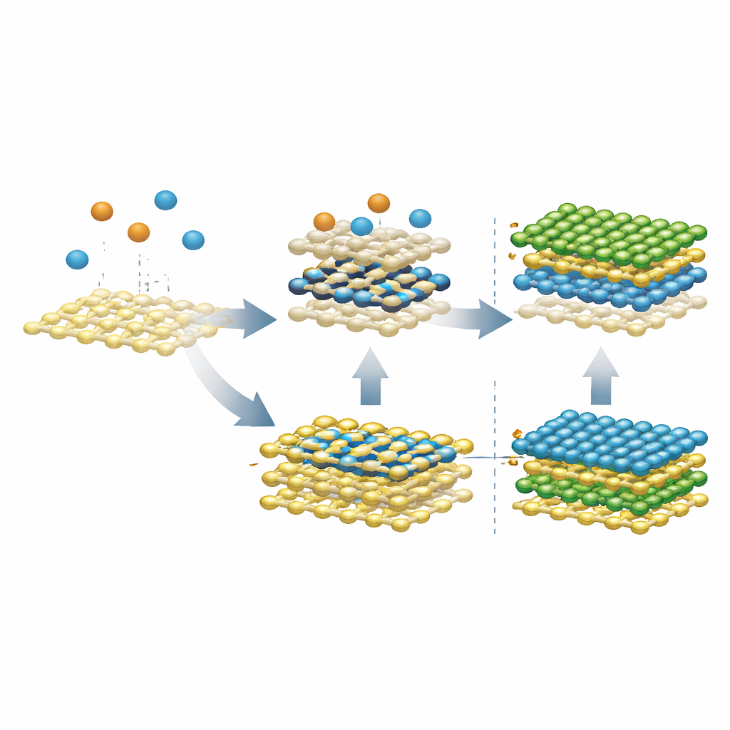
The simulations first looked at what happens when bare metal atoms land on an existing MoS2 or WS2 sheet, mirroring a two‑step vapor process used in experiments. Instead of remaining on top as a neat film, single molybdenum atoms quickly burrowed into the sulfur layer beneath the surface, forming a buried metal layer sandwiched between sulfur sheets—labeled SMoMoS when only molybdenum is involved, and SMMS when both molybdenum and tungsten mix. This sunken layer is surprisingly stable and encourages metal atoms in different positions to exchange, which naturally leads to alloying rather than a pristine MoS2/WS2 stack. At lower temperatures the exchange slows, but the tendency to sink remains, revealing why avoiding such intermediates is essential for clean heterostructures.
How extra sulfur protects the interface
The team then asked what happens when sulfur is introduced after this buried layer forms. When sulfur is added to the pure SMoMoS phase, it can drag molybdenum atoms back toward the surface and eventually rebuild a proper second MoS2 layer above the original sheet. However, when the buried layer is already an alloy (SMMS), the extra sulfur pulls both molybdenum and tungsten atoms upward, producing two alloyed layers instead of a sharp interface. Further simulations showed a way out: if incoming molybdenum arrives already bound to sulfur—forming Mo–S clusters instead of bare metal atoms—it no longer sinks. Under sulfur‑rich conditions, these clusters diffuse along the surface, merge and heal defects, allowing a clean second layer to grow without forming the troublesome buried alloy.
Turning a problem into a new kind of contact
Interestingly, the same buried metal layers that sabotage neat stacking may be extremely useful in their own right. Calculations show that SMoMoS and SMMS behave like metals and form low‑resistance p‑type contacts when joined to semiconducting MoS2. Unlike many conventional metal electrodes, which suffer from strong "pinning" effects that raise the barrier for holes, these coherent metal–metal interfaces keep that barrier small and tunable. This suggests that, if formed intentionally and in the right place, such intermediate layers could serve as ideal electrodes for ultrathin transistors.
What this means for atom-thin technology
Overall, the study reveals that the growth of stacked ultrathin materials is governed by a delicate balance between sinking bare metal atoms and stabilizing sulfur‑rich clusters on the surface. A specific buried metal layer, SMMS, emerges as the key gateway to unwanted alloying—but also as a promising metallic contact. For device makers, the message is simple: maintain sulfur‑rich conditions and avoid exposing existing layers to bare metal atoms if you want sharp interfaces, while deliberately creating buried metal layers where low‑resistance contacts are needed. By turning an invisible intermediate into a design parameter, this work offers a roadmap for both better fabrication and smarter use of two‑dimensional materials.
Citation: Zhao, L., Liu, H., Chang, Y. et al. Intermediates of forming transition metal dichalcogenide heterostructures revealed by machine learning simulations. Nat Commun 17, 3086 (2026). https://doi.org/10.1038/s41467-026-69977-x
Keywords: 2D materials, van der Waals heterostructures, machine learning simulation, MoS2 WS2 growth, contact engineering