Clear Sky Science · en
Conductive cobalt-based deposits grown by Cryo-FEBID for application as top-contact electrodes in large-area molecular electronic devices
Writing Tiny Wires with a Cold Beam
Modern electronics are built from patterns etched and printed onto chips, but shrinking devices further and wiring up individual layers of molecules is pushing today’s fabrication tools to their limits. This research shows how a “cold writing” method can quickly draw tiny, electrically conductive cobalt contacts exactly where they are needed, without damaging fragile molecular films underneath. The work brings molecular-scale circuitry a step closer to practical, large-area devices that might one day complement conventional silicon technology.
Why New Ways of Drawing Circuits Are Needed
Traditional chip-making tools rely on multiple processing steps, temporary resist layers and heating, all of which become slow, complex and sometimes unusable when features shrink to the nanoscale or when the underlying material is delicate. In molecular electronics, where a single layer of carefully arranged molecules carries current between two metal electrodes, the biggest headache is making the top contact: energetic metal atoms can punch through or rearrange the molecules, causing short circuits and ruining device performance. Softer alternatives exist, such as liquid metals or chemically formed contacts, but they are often hard to control in size and shape, making it difficult to design circuits with precise geometries.
A Cold, Direct-Write Approach
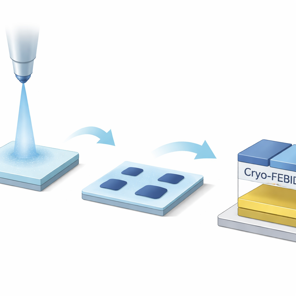
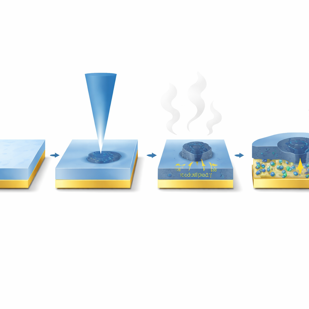
The technique explored here, called Cryo-FEBID, turns a focused electron beam into a nanoscale “pen.” First, the chip is cooled well below freezing and flooded with a vapor of a cobalt-containing molecule, which condenses into a thin frozen layer. When the narrow electron beam scans over selected regions, it breaks apart these molecules locally, leaving behind a cobalt-rich solid deposit. Afterwards, gentle heating removes the untouched frozen material, revealing a patterned cobalt structure written directly on the surface. Because the electrons have much lower momentum than ions or evaporated metal atoms, and because most of their energy is absorbed by the frozen layer, the process is far less damaging to anything buried beneath.
Making the Deposits Conduct and Controllable
The authors systematically tuned how these cobalt deposits grow and conduct electricity. By varying how far the gas nozzle sat from the sample, they adjusted the thickness of the frozen layer and thus the final deposit height. By changing the total electron dose, they altered the metal content and resistivity of the cobalt–carbon composite that forms. They found that above a certain dose the deposits behaved like good metals, with resistivity values comparable to other practical contact materials, while still being written in minutes over areas of tens to hundreds of square micrometers. Microscopy and chemical analysis confirmed that higher doses produced thicker, more uniform and more cobalt-rich structures without introducing large defects.
Gently Contacting a Single Layer of Molecules
To test whether this approach can truly make working molecular devices, the team built vertical “sandwich” structures consisting of a gold bottom electrode, a single molecular layer and a cobalt top contact grown by Cryo-FEBID. The molecules were chosen for their wire-like behavior and for chemical end-groups that bond well to cobalt, helping current pass across the interface. Atomic-force microscopy and surface measurements showed that the molecular layer was uniform and remained intact even after exposure to the electron beam and precursor gas. When the cobalt contacts were written on top, the resulting devices displayed the characteristic nonlinear current–voltage curves expected for such metal–molecule–metal systems, and the current scaled sensibly with contact area. About three-quarters of the devices worked as intended, a competitive yield for large-area molecular junctions.
Bringing Molecular Electronics Closer to Real Devices
Overall, the study demonstrates that cold, direct-write cobalt contacts can be grown quickly, conduct well and, crucially, leave underlying molecular layers functional over relatively large areas. For a general reader, this means that researchers are learning how to “wire up” sheets of molecules reliably enough to imagine integrating them with standard microelectronics. Because the same method can be steered anywhere on a chip and does not require masks, it could also be adapted to contact other sensitive materials, from atomically thin crystals to biological samples. By proving that Cryo-FEBID can produce conductive cobalt features without extra processing, the work broadens the toolbox for future nanoscale circuits that combine the precision of lithography with the unique properties of molecular and low-dimensional materials.
Citation: Salvador-Porroche, A., Gómez-González, A., Bonastre, J.M. et al. Conductive cobalt-based deposits grown by Cryo-FEBID for application as top-contact electrodes in large-area molecular electronic devices. Microsyst Nanoeng 12, 153 (2026). https://doi.org/10.1038/s41378-026-01280-7
Keywords: molecular electronics, nanofabrication, cobalt electrodes, cryogenic electron beam, top-contact junctions