Clear Sky Science · en
Ultrafast flash lamp annealing of magnetic tunnel junctions
A Faster Way to Build Tiny Magnetic Brains
Our phones, computers, and data centers increasingly rely on magnetic memory chips that remember information even when the power is off. These chips are built from stacks of ultrathin layers that must be “baked” at high temperature to work well, a step that is slow and energy hungry. This study explores a new kind of ultrafast light-based heating that can do the same job in seconds instead of hours, pointing toward quicker and more efficient manufacturing of future memory and sensor devices.
Why Magnetic Sandwiches Matter
At the heart of many advanced memory chips and ultra sensitive magnetic sensors lies a structure called a magnetic tunnel junction, which is essentially a tiny sandwich of metals and an insulating layer. The resistance of this sandwich changes depending on how the magnetic layers point, allowing the device to represent digital 0s and 1s. To reach the high performance needed in real products, the metallic layers must form an orderly crystal pattern guided by the central barrier layer. Conventional heat treatment in a furnace can achieve this order, but it typically requires temperatures of several hundred degrees Celsius held for hours, which slows down production and risks unwanted mixing of atoms between layers.
Flashes of Light Instead of Hours in a Furnace
In place of conventional furnace heating, the researchers used flash lamp annealing, where a powerful xenon lamp fires brief bursts of light lasting only thousandths of a second onto the chip surface. A sequence of these pulses can briefly raise the top of the wafer to temperatures that simulations suggest can exceed 1000 degrees Celsius, while the supporting holder warms only modestly and cools quickly. By varying the number of pulse groups, the team controlled the total heating time from fractions of a second to a few seconds. They found that with just over one and a half seconds of total light exposure, the magnetic tunnel junctions achieved a change in resistance nearly as large as that produced by several hours of traditional heating, even though the overall heat dose was far smaller. 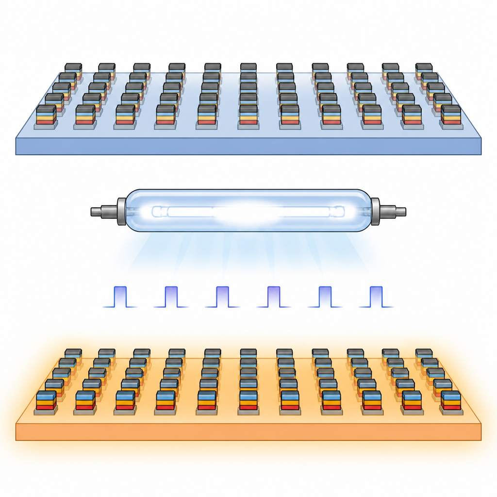
Looking Inside the Layers
To see what these flashes were doing to the tiny layers, the team used high resolution electron microscopes and chemical mapping tools. In untreated devices the key magnetic layers were amorphous, meaning the atoms had no regular pattern, and the memory effect was weak. After long furnace treatment the layers became neatly ordered, and a light element called boron moved significantly out of the magnetic layers into neighboring layers, a change known to favor strong electronic tunneling between the magnets. With the optimized flash lamp condition, the upper magnetic layer crystallized well, while the lower one crystallized only near its interface with the barrier. Chemical maps showed that, compared with furnace heating, less boron had escaped from the magnetic layers during the brief flashes, reflecting the much shorter heating time.
Finding the Sweet Spot
Increasing the number of light pulses further continued to change the internal structure. The lower magnetic layer eventually crystallized almost completely, even though the boron concentration around it stayed relatively high, suggesting that the timing of ordering and diffusion follows different clocks. But when the flashing became too strong, oxygen began to creep into metallic regions and the clean separation between layers started to blur. In this case the memory performance dropped and electrical resistance rose, likely because key layers partially oxidized or mixed. These trends show that there is a narrow window of flash conditions that balance fast ordering of atoms, limited chemical mixing, and avoidance of damage.
What This Means for Future Electronics
The study shows that well performing magnetic tunnel junctions can be prepared in about 1.7 seconds of flash lamp treatment, compared with hours of conventional heating, while keeping unwanted atomic diffusion in check. With further tuning of pulse strength and spacing, this approach could shorten manufacturing time and cut the energy cost of processing magnetic memory and sensor chips, and may allow such devices to be built on heat sensitive or flexible substrates. In simple terms, the work suggests that a controlled burst of light can do much of the careful “baking” that these tiny magnetic sandwiches need, opening a path toward faster, more versatile spin based electronics. 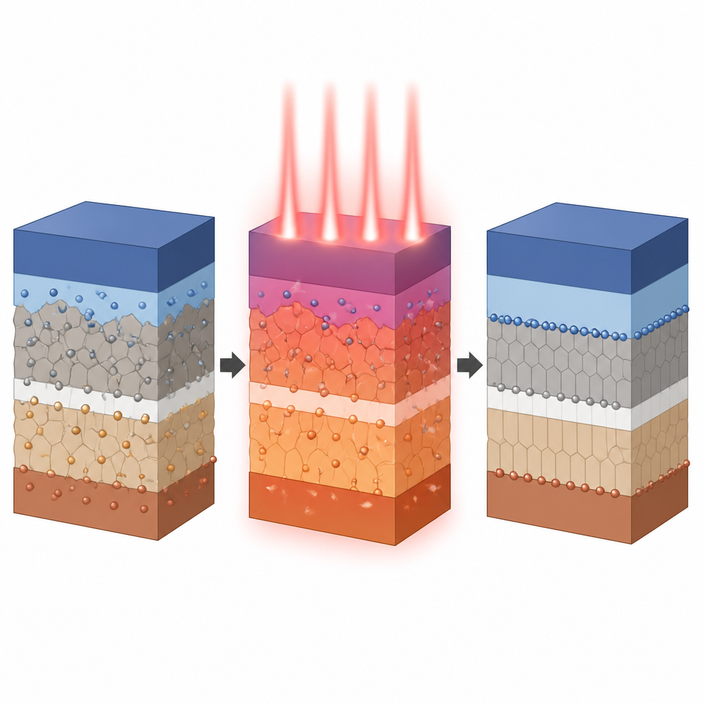
Citation: Imai, A., Ota, S., Yamasaki, J. et al. Ultrafast flash lamp annealing of magnetic tunnel junctions. npj Spintronics 4, 20 (2026). https://doi.org/10.1038/s44306-026-00145-z
Keywords: flash lamp annealing, magnetic tunnel junctions, MRAM, spintronics, rapid thermal processing