Clear Sky Science · en
3D reconstruction and etching profile simulation for wiggling active area effect in dynamic random access memory manufacturing
Why tiny wiggles matter for everyday computing
Every time you open an app, stream a video, or run a game, your device leans heavily on a workhorse technology called DRAM, the main memory inside computers and phones. As companies pack more bits of information into each chip, the tiny 3D structures that store and move electric charge must be etched with extreme precision. In this study, researchers tackled a puzzling defect nicknamed the “wiggling active area,” where key transistor features in DRAM bend and bulge instead of staying straight. Understanding and controlling this subtle distortion could help keep future memory chips fast, efficient, and reliable.
The problem inside next‑generation memory chips
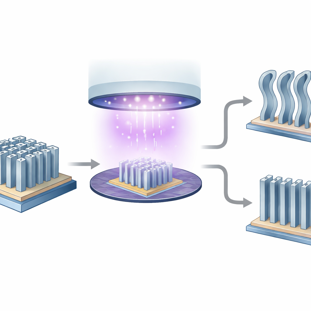
Modern DRAM cells rely on narrow, fin-like regions called active areas, which act as the highway for charge to flow in and out of tiny capacitors that store data. To reach the enormous densities demanded by today’s electronics, chipmakers pattern these fins using sophisticated, multi-step approaches. However, when the fins are carved out of silicon using plasma etching—a process that bombards the surface with energetic particles—their originally straight shapes can warp into gently wavy or leaning profiles. These “wiggling” fins reduce how well capacitors can charge and discharge and can eventually undermine the reliability of entire memory arrays. The effect has been widely seen in industry, but its detailed physical origin remained unclear.
Seeing the full 3D shape of nanoscale fins
Traditional imaging tools such as scanning and transmission electron microscopes mostly provide flat, two-dimensional snapshots. For intricate, deep structures like DRAM active areas, that is like judging a skyscraper from a single floor plan. The team instead used a method called FIB-SEM, which alternates between shaving off ultrathin layers of material with an ion beam and imaging each layer with an electron microscope. By stacking about 300 such images and processing them with advanced software and deep-learning-based segmentation, they reconstructed a full three-dimensional view of the fins etched under one set of conditions. These reconstructions revealed that the wiggling effect grows stronger with depth and that the fins broaden and curve more near their bottoms, confirming hints seen in simple cross-section images but now mapped in full 3D detail.
Building a virtual etching lab in the computer
While 3D reconstruction delivers rich detail, it is slow, destructive, and impractical to repeat for many different process recipes. To explore what causes the wiggling and how to control it, the researchers built a three-dimensional computer model of the etching process. Using a Monte Carlo approach, they treated the material as tiny volume elements and simulated streams of neutral particles and ions striking the surface, reacting, and removing or depositing material. Their model captured how particle flux, surface reactions, and reflections shape the evolving fin profile over time. They then ran virtual experiments matching their lab conditions, especially focusing on three oxygen flow rates in the etch gas mixture: low, medium, and high.
How oxygen flow turns straight fins into wavy ones
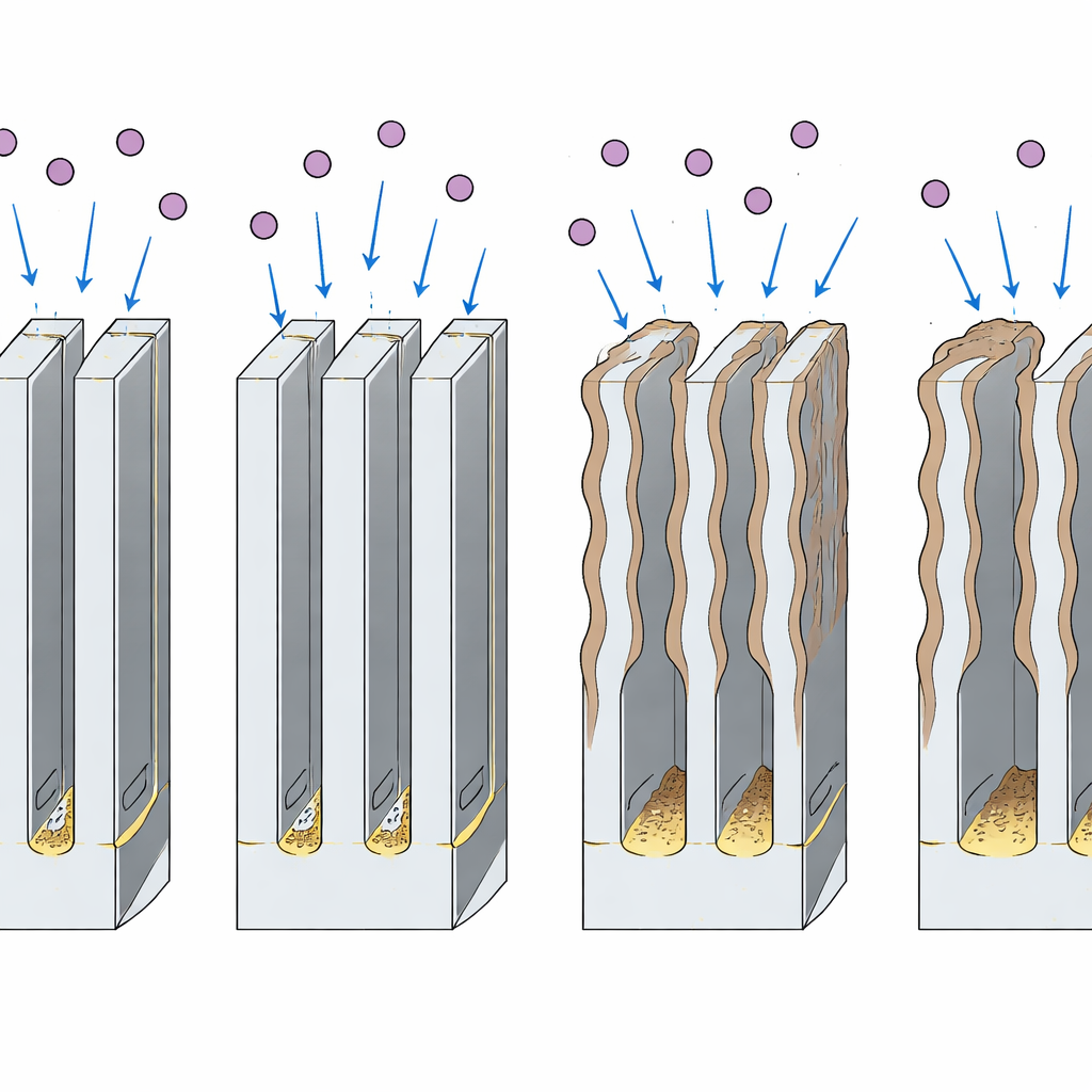
The simulations closely mirrored the 3D reconstructions. As the oxygen flow increased, the fins became more tapered and more strongly wiggled along their height, just as in the real experiments. The model exposed a key mechanism: a “loading effect,” where regions with wider openings between fins receive more reactive species and form different amounts of by-products on their sidewalls than narrow regions. In the bromine-and-oxygen chemistry used here, volatile silicon-bromine compounds and oxygen-driven surface layers together govern how fast the bottom etches and how much protective film builds up on the sides. More oxygen encourages thicker sidewall protection and redeposition, which in turn amplifies the sideways growth and waviness of the fins. To quantify this, the team defined a simple “wiggling degree” based on how much the fin width grows compared with its original patterned size; this metric consistently increased with higher oxygen flow, in both experiments and simulations.
A clearer path to better memory manufacturing
By combining high-resolution 3D imaging with a carefully calibrated 3D simulation, the study connects a long-observed industrial defect to concrete, controllable process knobs. The results show that wiggling active areas are not just the result of flawed masks at the surface but can be generated deep within the etch itself through the way gases, ions, and by-products interact in crowded nanoscale spaces. Lowering the oxygen flow during etching was shown to reduce the severity of the wiggles, offering a practical guideline for chip manufacturers, while also hinting at trade-offs that future work must explore. In essence, the authors provide both a diagnostic toolkit and a design map for etch recipes that keep DRAM fins straighter—and our everyday digital devices running smoothly.
Citation: Hu, Z., Wen, J., Yang, C. et al. 3D reconstruction and etching profile simulation for wiggling active area effect in dynamic random access memory manufacturing. Commun Eng 5, 65 (2026). https://doi.org/10.1038/s44172-026-00626-3
Keywords: DRAM manufacturing, plasma etching, 3D nanostructures, process simulation, semiconductor reliability