Clear Sky Science · en
Giant Rashba splitting in a 2D BiAs layer on InAs(111)B
Why tiny layers can reshape future electronics
Modern gadgets increasingly rely on not just the flow of electric charge, but also on the spin of electrons, a quantum property that can act like a tiny compass needle. Materials that let engineers generate and steer these spins efficiently are key for low‑power computers, fast memory and quantum devices. This study reports how a sheet only a few atoms thick, made from bismuth and arsenic and grown on an indium arsenide crystal, can host unusually strong spin effects and how a clever protective coating is crucial to make this fragile structure stable and usable.
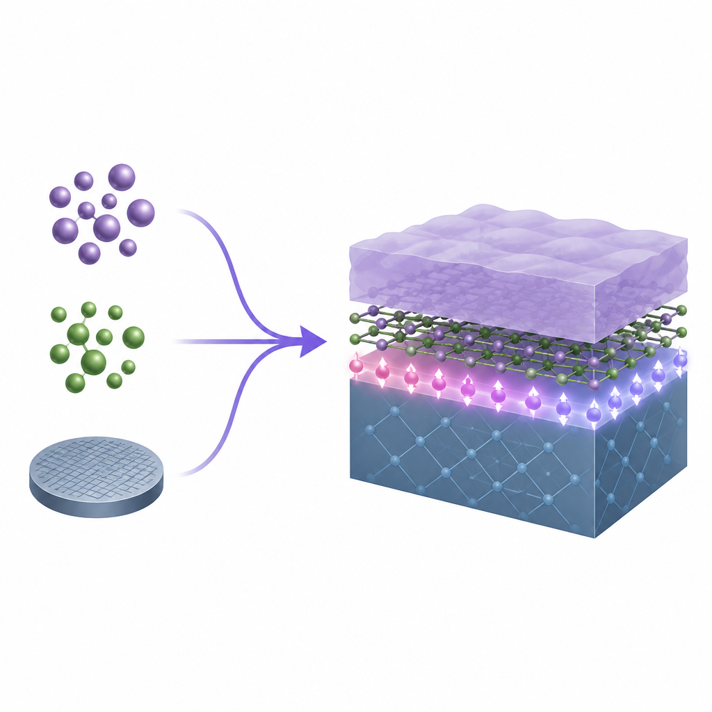
Building a new ultra thin material
The researchers started with a semiconductor called indium arsenide, already valued for its fast electrons and use in infrared sensors and advanced transistors. They used a method known as molecular beam epitaxy to gently deposit a tiny amount of bismuth onto a carefully cleaned indium arsenide surface, then covered everything with a glassy layer of arsenic. By slowly removing most of this top layer in vacuum, they exposed a two‑dimensional sheet of bismuth arsenide, or BiAs, that had formed right at the surface of the crystal. Several surface probes, including patterns formed by low‑energy electrons and images from a scanning tunneling microscope, showed that this new layer could adopt a simple, orderly arrangement when the arsenic coating was still partly in place.
Probing the hidden landscape of electrons
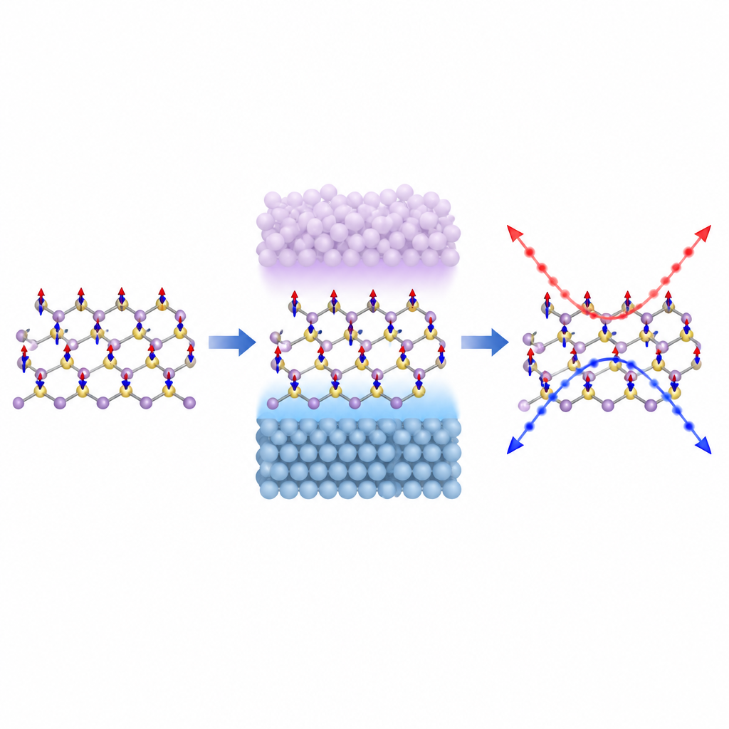
To see how electrons move in this stacked structure, the team used angle‑resolved photoemission spectroscopy, which maps out the allowed energies and momenta of electrons. Compared with bare indium arsenide, the surface with the BiAs layer displayed a dramatic new signature in these maps: a distinctive "M"‑shaped feature and a small pocket of electron states right at the energy level where electrical conduction begins. These changes signaled that the thin BiAs sheet was not just sitting passively on the surface, but was creating new quantum states that could be harnessed for devices that rely on electron spin.
How a subtle structural shift boosts spin control
The team turned to computer simulations based on density functional theory to understand how atoms in the BiAs layer are arranged and why that matters for spin behavior. They compared two possibilities for where bismuth atoms sit relative to the atoms in the underlying crystal. In one case, the BiAs layer simply continues the same pattern as the substrate. In the other, it is slightly shifted sideways. The calculations showed that when an arsenic overlayer is present, this shifted arrangement becomes more stable. Crucially, only this displaced structure supports a strong Rashba effect, in which the combination of heavy atoms and a built‑in asymmetry causes electron spins moving in opposite directions to separate in space.
Protective cap that quietly sets the rules
The glassy arsenic coating turned out to be more than just a protective cover. It locks in the sideways shift between the BiAs layer and the indium arsenide substrate, while preventing the surface from rearranging into a more complex pattern that would erase the special electronic states. When the researchers heated the sample further and drove off nearly all of the arsenic overlayer, the surface reorganized into a new structure. Microscopy and diffraction showed a different symmetry, and the striking M‑shaped feature in the electron maps almost disappeared, even though bismuth was still present. This contrast highlighted how strongly the protective cap controls the delicate balance between structure and spin behavior.
What this means for future spin based devices
From the combination of experiments and theory, the authors conclude that the BiAs sheet on indium arsenide belongs to a family of so‑called giant Rashba materials, where the separation of spin states is especially strong. In plain terms, the system can create and manipulate streams of electrons whose spins point in opposite directions, a key ingredient for spintronics and some quantum information schemes. Just as important, the work demonstrates a practical recipe: use a simple elemental overlayer to stabilize exotic two‑dimensional compounds that might otherwise fall apart. This strategy could be extended to other bismuth‑rich materials, opening new paths toward energy‑efficient transistors, magnetic memories and light‑emitting devices that all exploit the spin of the electron as well as its charge.
Citation: Benter, S., Da Paixao Maciel, R., Plissard, S. et al. Giant Rashba splitting in a 2D BiAs layer on InAs(111)B. Commun Mater 7, 123 (2026). https://doi.org/10.1038/s43246-026-01185-y
Keywords: Rashba splitting, spintronics, 2D materials, bismuth arsenide, indium arsenide