Clear Sky Science · en
Electronic localization and optical activity of strain-engineered transition-metal dichalcogenide nanobubbles
Stretching Tiny Sheets for Quantum Light
Imagine peeling off an ultra-thin sheet of semiconductor—just a single layer of atoms—and gently puffing it up into a tiny bubble. Physicists hope that these nanobubbles can act like man‑made "atoms" that emit single particles of light on demand, a key ingredient for future quantum technologies. This study uses advanced computer simulations to test that idea for a popular family of two‑dimensional materials and asks a simple but crucial question: can perfect, tiny bubbles made only by stretching the sheet really shine the way we want?
What These Atom-Thin Bubbles Are
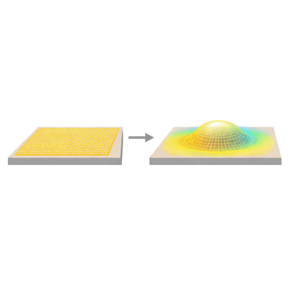
The work focuses on transition‑metal dichalcogenides—atomically thin crystals such as MoS2 and WSe2 that behave like ultrathin semiconductors. Experiments have shown that when these sheets blister into nanobubbles, their electrons can become trapped in small regions, which is promising for creating quantum light sources. However, real samples also contain defects, irregular shapes, and substrates, making it hard to pinpoint what pure mechanical stretching alone can do. The authors therefore build idealized bubbles on the computer: perfectly clean, free‑standing sheets gently inflated by well‑controlled forces, small enough (below ten nanometers across) that quantum confinement and extreme curvature should be most pronounced.
How Stretching Changes Shape and Strain
Using first‑principles quantum calculations, the team simulates 36 different bubbles made of four materials (MoS2, WS2, MoSe2, WSe2) while gradually increasing the inflating force. As the sheets bulge upward, their shapes respond differently depending on the chemical makeup: some materials form taller, softer domes, while others stay flatter and stiffer. The stretching is not uniform. Tensile strain—atoms pulled apart—concentrates near the bubble’s apex, while a ring of compressed material forms around it and additional strain appears near the pinned edges. This highly uneven strain pattern turns out to be a recurring feature across all materials and is the starting point for understanding how electrons and holes behave inside the bubble.
Trapped States Without Bright Light
On the electronic level, inflation systematically narrows the energy gap between filled and empty states, a key quantity that controls how the material absorbs and emits light. More strikingly, the stretching creates a special, nearly flat electronic state in the valence region in every type of bubble. "Flat" means that the energy of this state barely changes with electron momentum, a hallmark of strong localization in real space: the corresponding wave function piles up near the bubble apex, mimicking a quantum dot. For bubbles made of MoS2 and WS2, this localized state can even be pushed into the material’s gap, becoming the highest occupied state; for MoSe2 and WSe2 it stays slightly lower but still lies close in energy. Meanwhile, the lowest empty states remain spread out over the entire sheet and prefer a different region of momentum space.
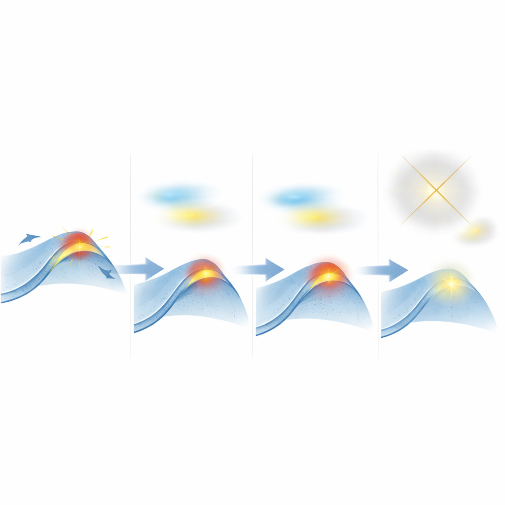
Why the Supposed Quantum Dot Stays Dim
To test whether these localized states actually support bright optical transitions, the authors calculate how strongly they couple to light. Despite looking ideal from a confinement perspective, transitions starting from the apex‑localized state to the lowest empty states are almost always dark or extremely weak, regardless of material. By unfolding the complex band structure of a representative bubble back into that of a flat monolayer, the study shows why: the localized valence state lives mainly at one special momentum point (Γ), whereas the conduction minimum remains near another (K). Because ordinary light absorption and emission favor transitions that conserve momentum, this mismatch strongly suppresses the relevant processes. In effect, the bubble does create a quantum‑dot‑like trap, but one that is poorly connected, optically, to the states that usually dominate light emission in these materials.
What This Means for Future Quantum Devices
In everyday terms, the study finds that simply puffing up a perfect, tiny bubble in an atom‑thin semiconductor is not enough to make a bright single‑photon source. Strain alone can engineer localized electronic states and reshape the energy landscape, but the key transitions from those states to the main light‑emitting channels remain largely forbidden by momentum‑space rules. The authors conclude that the strong quantum emission seen in larger, real‑world bubbles likely depends on additional ingredients—defects, sharper deformations, substrate effects, or local electric fields—that relax these rules and create deeper or better‑connected traps. Their work provides a clear baseline: it shows what pure, strain‑engineered nanobubbles can and cannot do, offering design principles for more realistic structures aimed at quantum technologies.
Citation: Velja, S., Steinhoff, A., Krumland, J. et al. Electronic localization and optical activity of strain-engineered transition-metal dichalcogenide nanobubbles. npj 2D Mater Appl 10, 53 (2026). https://doi.org/10.1038/s41699-026-00702-4
Keywords: 2D materials, strain engineering, nanobubbles, quantum emitters, single-photon emission