Clear Sky Science · en
Water-based, large-scale transfer of 2D materials grown on sapphire substrates
Moving Atom-Thin Materials Safely
Electronics of the future may be built from sheets of material only a few atoms thick, promising ultra-fast, low-power chips and sensors. But there is a practical problem: many of these fragile films must be grown at very high temperatures on special crystals, then gently moved onto the cooler, more common silicon wafers used in industry. This paper describes a surprisingly simple way to move such atom-thin layers using nothing more exotic than purified water and a plastic frame.
Why Ultra-Thin Layers Matter
Two-dimensional materials such as molybdenum disulfide (MoS2) and hexagonal boron nitride (h-BN) are just a few atoms thick yet can act as excellent semiconductors or insulators. They are promising building blocks for new kinds of transistors, memory elements, and light-based devices. Today they are often grown on sapphire, a hard, transparent crystal that tolerates high heat and helps the material arrange itself in an orderly fashion. However, modern chip factories rely on silicon wafers, and the high temperatures needed for growth on sapphire do not fit easily into standard production lines. A reliable way to peel these delicate films off sapphire and place them onto silicon, without damage, is therefore essential.
The Trouble with Harsh Chemicals
Traditional transfer methods use strong chemicals such as potassium hydroxide (KOH) to etch or weaken the bond between the thin film and its sapphire base. Researchers typically coat the film with a protective plastic, then hold the sample by hand in a chemical bath and “fish” the floating film onto a new substrate. This approach is fiddly and risky: it demands steady hands and protective gear, can lead to folds and tears in the film, and may even alter the microscopic structure of the material. Since these atom-thin layers are extremely sensitive to their environment, chemical exposure can introduce defects, extra crystal grains, or unwanted electrical charges that undermine device performance.
Letting Water Do the Work
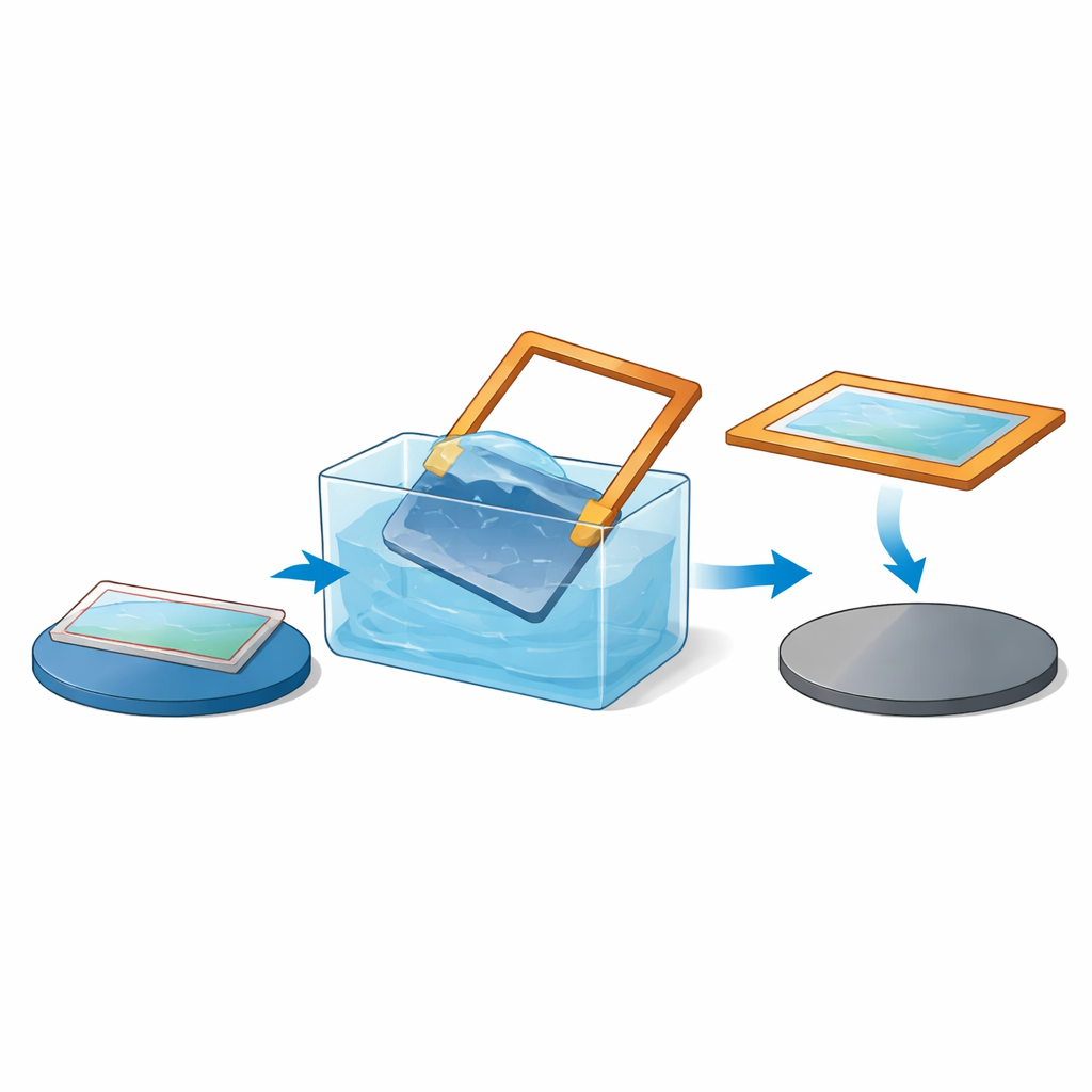
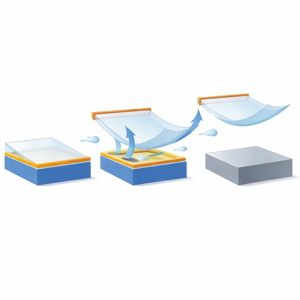
The authors build on theoretical work suggesting that when both the sapphire and the two-dimensional material attract water, liquid can slip into the tiny gap between them and help pry them apart. They first coat the material with a thin plastic support and attach a simple frame made from adhesive tape and plastic foil. Mounted at a slight angle in a beaker or tub, the framed sample is slowly flooded with deionized (highly purified) water. The water’s surface tension makes the frame float and gently tug upward on the plastic-supported film, while individual water molecules creep into the interface with the sapphire. Over minutes, this combined action cleanly peels the entire film from the crystal, leaving it floating on the water surface. The floating sheet can then be guided onto a silicon wafer, dried, and freed from its plastic support, all without using acids or bases.
Checking the Film Under the Microscope
To test whether this gentle-looking method truly preserves material quality, the team examined the films before and after transfer using several high-resolution tools. Atomic force microscopy and electron microscopy showed that the surface of h-BN remained smooth, with no significant increase in particles or damage; its characteristic layered structure was intact when viewed atom-by-atom in a transmission electron microscope. For MoS2, the tiny crystal grains and vertical nanosheets created during growth were still present, and only a slight increase in nanoscale particles—likely plastic residue—was seen. Detailed light-scattering measurements (Raman and photoluminescence) revealed that both materials experienced a release of built-in compressive strain once moved off sapphire, but did not show signs of extra defects or harmful doping. In other words, the films relaxed mechanically without losing their electronic quality.
From Small Chips to Full Wafers
Crucially, the researchers pushed the technique beyond small test pieces to full wafers. They successfully transferred MoS2 grown on a 100 mm sapphire wafer onto a larger silicon wafer coated with oxide, using the same water-based approach and a larger frame and support mount. Mapping the film’s properties over a wide area showed nearly complete coverage—about 99.7%—with only a handful of tiny gaps or measurement failures. The overall signature of reduced internal stress and preserved material quality matched the results from smaller samples, suggesting the method is robust and scalable to sizes relevant for industry.
Gentle Peeling for Future Chips
In everyday terms, this work shows that a carefully designed “water lift” can move ultrathin, fragile materials from one solid surface to another without harsh chemicals or complex handling. By using surface tension and a mechanical frame, the process peels the films cleanly, allowing them to relax and settle onto silicon with little damage. This environmentally friendlier and safer approach could ease the integration of next-generation atom-thin materials into mainstream chip manufacturing, bringing laboratory demonstrations a step closer to practical, large-scale electronic and memory devices.
Citation: Rademacher, N., Völkel, L., Reato, E. et al. Water-based, large-scale transfer of 2D materials grown on sapphire substrates. npj 2D Mater Appl 10, 48 (2026). https://doi.org/10.1038/s41699-026-00696-z
Keywords: two-dimensional materials, water-based transfer, molybdenum disulfide, hexagonal boron nitride, sapphire to silicon