Clear Sky Science · en
Strain-tunable inter-valley scattering defines universal mobility enhancement in n- and p-type 2D TMDs
Stretching Atom-Thin Semiconductors
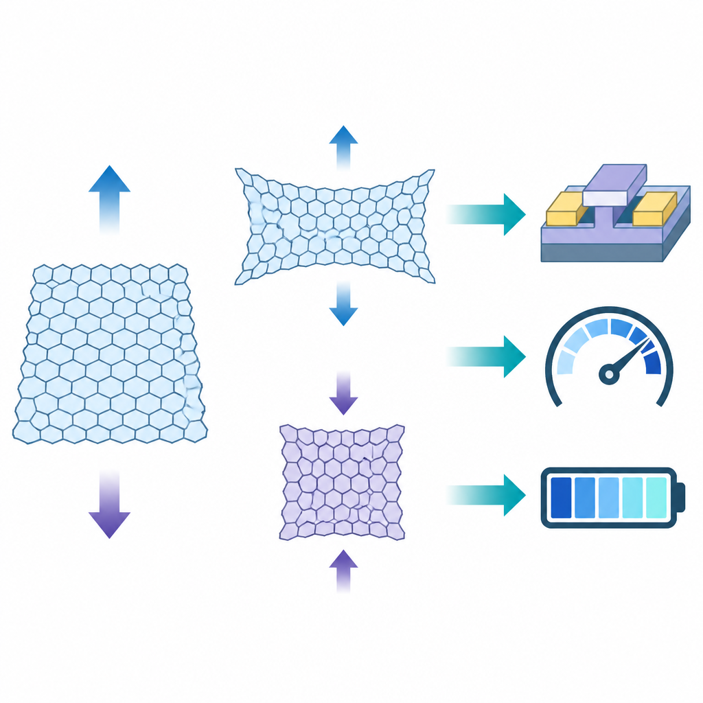
Our smartphones, laptops, and data centers all rely on tiny switches called transistors. As engineers push these switches to be ever thinner, traditional silicon begins to struggle. This study explores a new class of atom-thin semiconductors, known as 2D transition metal dichalcogenides, and shows how gently stretching or squeezing them can make electric charges flow more easily, paving the way for faster and more efficient electronics.
Why Thin Crystals Need a New Approach
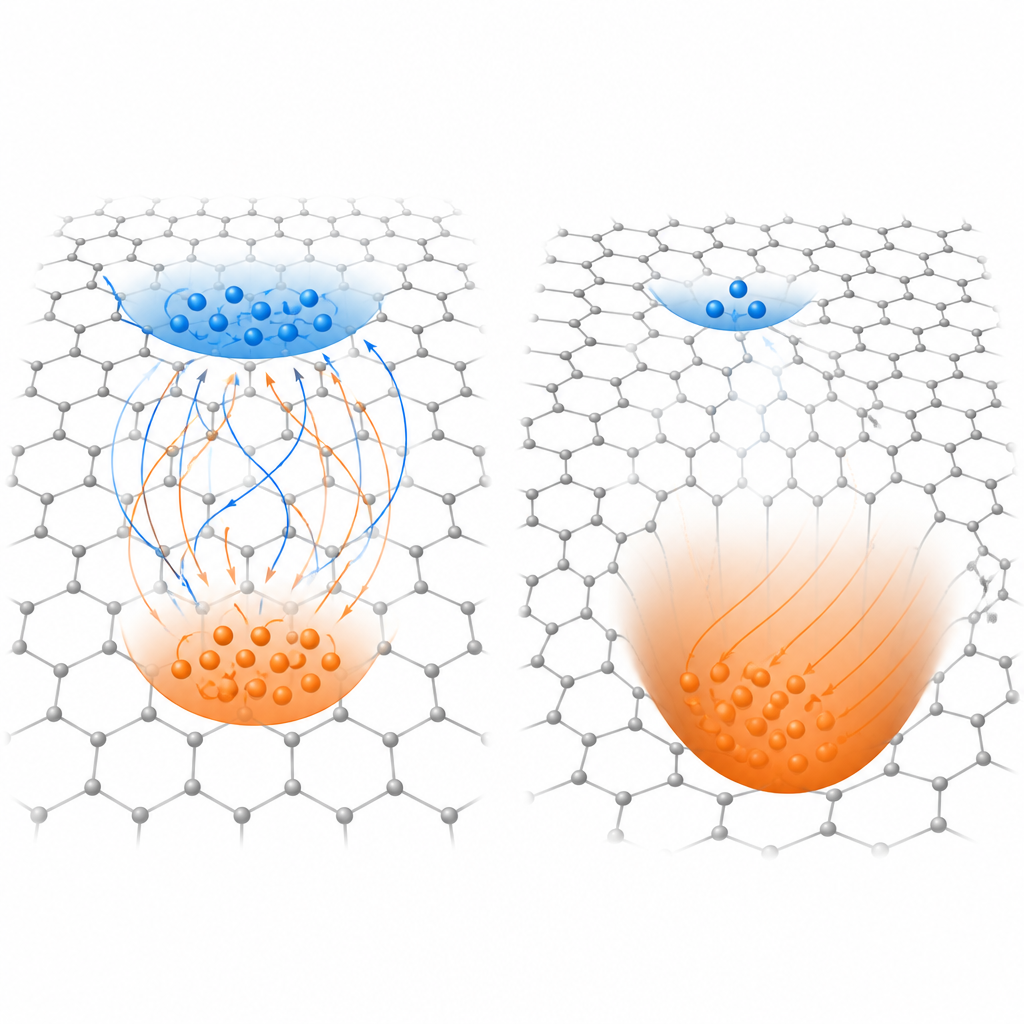
Conventional semiconductor chips are built from thick crystals where strain mainly changes how heavy or light charge carriers appear to be. In atom-thin layers, the story is different. These materials host several "valleys" in their energy landscape, each acting like a different lane for electrons or holes. The ease with which charges jump between these valleys strongly affects how quickly they can move through a device. The authors argue that in these 2D crystals, tuning this inter-valley hopping with strain matters far more than the traditional focus on effective mass used for bulk silicon.
How the Team Probed the Invisible Landscape
To uncover what strain really does, the researchers built a multiscale model that starts from the quantum behavior of atoms and works up to the performance of full devices. They used first-principles calculations to map out how the electronic bands and vibrations of several popular 2D materials change as the crystal is uniformly stretched or compressed. These results feed into a transport model that tracks how electrons and holes scatter off vibrations, charged impurities, and remote vibrations in nearby insulating layers, allowing the team to calculate how mobility responds to strain under realistic operating conditions.
What Happens When You Stretch Electron Materials
For electron-carrying (n-type) materials such as MoS2, MoSe2, and WS2, the key competition is between two valleys called K and Q. In an unstrained sheet, both valleys contribute to conduction, and electrons can scatter back and forth between them, slowing overall motion. When the sheet is placed under gentle tensile strain, the K valley moves lower in energy while Q moves higher, widening the gap between them. This makes it much harder for electrons to hop into the less favorable valley, sharply reducing inter-valley scattering. The result is a marked rise in mobility, with WS2 showing the strongest improvement. Even when real-world nuisances like charged dirt at interfaces and vibrations coming from the underlying oxide are included, the relative boost from strain remains large.
How Squeezing Helps Hole Materials
For hole-carrying (p-type) materials such as MoSe2, WSe2, and MoTe2, the important valleys sit at different points, labeled Γ and K. Here, compressive strain rather than tensile strain is the hero. Pushing the sheet inward pulls the heavier Γ valley away in energy while favoring the lighter K valley. Once again, this increases the energy barrier for holes to jump between valleys, cutting down inter-valley scattering. Among the hole materials, WSe2 stands out for combining a stiff lattice with relatively weak coupling to vibrations, giving it both high baseline mobility and the largest gains under compression. The study shows that these benefits persist over practical ranges of temperature, charge density, impurity level, and choice of surrounding dielectric.
From Models to Future Devices
To test their framework, the authors compared their calculated unstrained mobilities and strain responses against many experimental measurements and found close agreement for several materials and device layouts. Their central message is that carefully applied strain offers a reliable knob to enhance mobility in both electron and hole channels of 2D devices, with improvement rates that surpass what has been achieved in silicon. For chip designers, this means that pairing high-quality 2D crystals with suitable insulating layers and controlled amounts of stretch or compression could unlock faster, lower-power transistors built from just a few atomic layers.
Citation: Afrid, S.M.TS., Zhao, H.L., van der Zande, A.M. et al. Strain-tunable inter-valley scattering defines universal mobility enhancement in n- and p-type 2D TMDs. npj 2D Mater Appl 10, 57 (2026). https://doi.org/10.1038/s41699-026-00689-y
Keywords: 2D materials, strain engineering, carrier mobility, transition metal dichalcogenides, nanoelectronics