Clear Sky Science · en
Oxide induced degradation in MoS2 field-effect transistors
Why ultra-thin electronics can suddenly slow down
As our phones, laptops, and data centers keep shrinking and speeding up, engineers are looking to exotic, sheet-like materials only a few atoms thick to build the next generation of transistors. One star candidate is molybdenum disulfide (MoS2), a two-dimensional semiconductor. Yet when MoS2 is integrated into realistic devices, its performance often falls far short of what its raw material properties promise. This paper digs into a hidden culprit at the heart of that mystery: the messy, disordered oxide layers that surround the MoS2 channel in practical chips.
The promise of atom-thin switch components
Two-dimensional materials are crystals that can be peeled down to a single atomic layer, offering excellent control of current in extremely small transistors. In theory, single-layer MoS2 should have higher mobility—that is, electrons should move through it more easily—than thicker versions with two or three layers. It should also resist short-channel effects, the leakage and loss of control that plague ever-smaller silicon devices. But in actual integrated circuits, the opposite trend is often observed: devices with thicker MoS2 channels behave better than those using the thinnest layers, suggesting that something outside the MoS2 itself is holding it back.
When the surrounding material becomes the problem
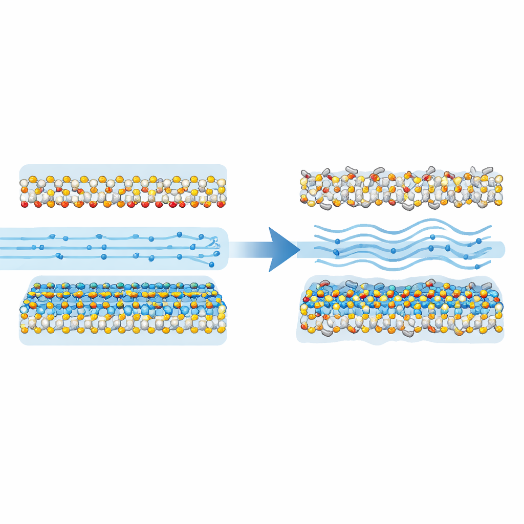
The key suspect is the gate oxide, the insulating material placed directly above and below the MoS2 to allow the gate electrode to switch the transistor on and off. In silicon technology, a thin, high-quality native oxide forms a clean, uniform interface. For MoS2, however, engineers often must rely on amorphous, or structurally disordered, oxides such as aluminum oxide (Al2O3) and hafnium oxide (HfO2). Using large-scale quantum mechanical simulations that require no empirical fitting, the authors explicitly built atomic models of MoS2 in contact with these amorphous oxides and then simulated full transistor behavior. This let them connect specific atomic-scale features—like missing atoms and uneven surfaces—to macroscopic device properties such as current, leakage, and switching sharpness.
Invisible bumps and traps that block electrons
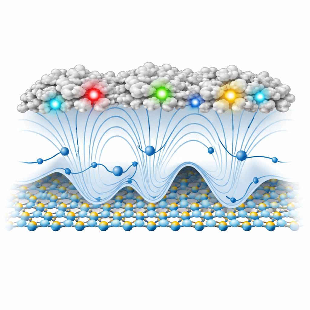
The study reveals two main ways in which amorphous oxides undermine MoS2 transistors. First, defects in the oxide, especially missing oxygen atoms, create localized electronic states inside the MoS2 band gap. These "trap" states can grab and release electrons and also serve as intermediate stepping stones for current to tunnel from source to drain even when the transistor is supposed to be off, boosting unwanted leakage. Second, the irregular chemical makeup and roughness of the oxide surface cause certain electronic orbitals of the oxide and MoS2 to mix. Together, these defects and hybridized regions generate a patchwork of electrostatic "hills" and "valleys" inside the MoS2 layer. Electrons moving along the channel are scattered by these potential fluctuations, which lowers mobility, reduces the maximum switch-on current, and makes the subthreshold swing—the sharpness of turn-on—worse.
Why thicker layers cope better with bad surroundings
By simulating devices with one, two, and three MoS2 layers, the authors show that the thinnest channels suffer most: as the material gets thinner, it feels the oxide’s irregularities more strongly, leading to larger potential fluctuations and stronger performance loss. In monolayer devices, mobility at operating gate voltage can drop by roughly 70 percent compared with the same structure using an ideal crystalline oxide; for trilayer MoS2, the reduction is closer to 40 percent. This matches experimental reports where thicker MoS2 channels often outperform monolayers once real gate stacks are included. However, the work also identifies a promising path forward: if the amorphous oxide surface is well passivated with hydrogen, free of oxygen vacancies, and chemically uniform, a monolayer device can still retain up to about 80 percent of the current of a device using a nearly perfect crystalline oxide.
What this means for future tiny chips
For non-specialists, the take-home message is that the limiting factor for tomorrow’s ultra-thin transistors may not be the exotic channel material itself, but the seemingly mundane oxide that surrounds it. Atomic-scale disorder and defects in these oxides create invisible energy landscapes that slow, scatter, and leak electrons in MoS2 devices, especially when the channel is only a single layer thick. The simulations show that by engineering cleaner, more uniform oxide interfaces—either through better materials, defect control, or interfacial layers—engineers can unlock much more of the intrinsic potential of two-dimensional semiconductors. In other words, making the "insulating" parts of the device nearly perfect is just as critical as choosing the right ultrathin conductor.
Citation: Ducry, F., Van Troeye, B., Dossena, M. et al. Oxide induced degradation in MoS2 field-effect transistors. npj 2D Mater Appl 10, 49 (2026). https://doi.org/10.1038/s41699-026-00677-2
Keywords: 2D materials, MoS2 transistors, gate oxides, device degradation, interface defects