Clear Sky Science · en
Sustained poling-induced second-order optical nonlinearity in sodium-doped amorphous niobium oxide waveguides
Why shaping light on a chip matters
Many of today’s communication and sensing technologies depend on tiny structures that guide and sculpt light on a chip. Devices that can quickly change or convert light signals are usually built from crystalline materials that are powerful but difficult to shape. This study explores a more flexible glass-like material that can be “written” with special regions where light behaves in a highly tunable way, opening a path to smaller, more easily manufactured optical circuits.
From stiff crystals to flexible glass films
For decades, lithium niobate crystals have been the workhorse material for devices such as high speed light modulators and frequency converters. They owe their success to a strong effect in which light at one color can generate light at a new color inside the crystal. However, these crystals are hard, chemically resistant, and direction dependent, which makes them challenging to carve into intricate waveguides with tight bends. The authors look instead at thin glassy films of niobium oxide that contain sodium. Unlike a crystal, this material has no preferred direction, and can be deposited as a uniform layer on glass, making it much easier to pattern with standard chip making tools.
Writing active zones into a glass film
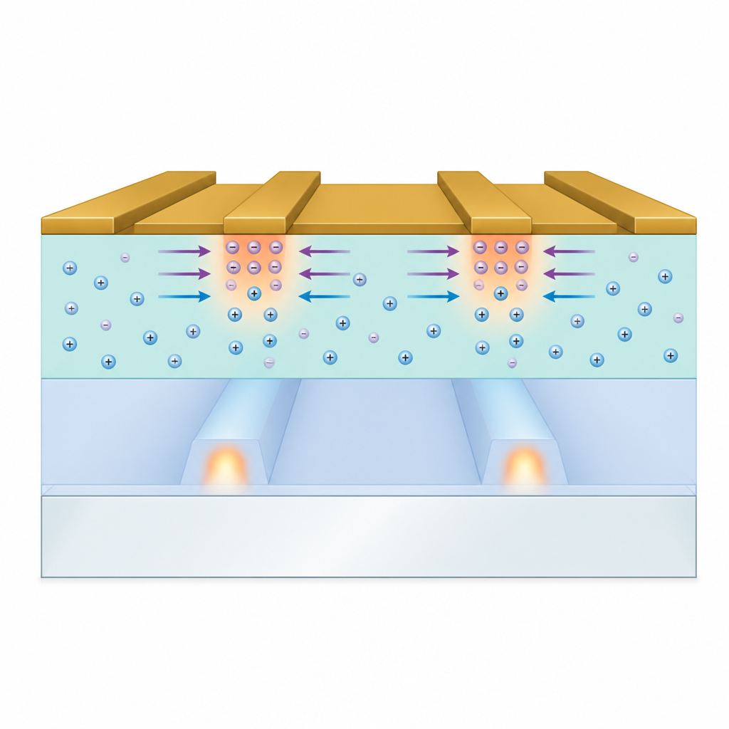
On their own, these amorphous films do not show the special light mixing effect. The team activates them using a process called thermal poling, in which a patterned metal electrode is placed on the film, a strong voltage is applied, and the stack is heated. Under these conditions, charged atoms in the film slowly drift, freezing in a built in electrical field once the sample cools. Using a microscope that measures faint green light generated from an infrared laser beam, the researchers map where the new effect appears. They find that the light mixing is strongest in narrow bands close to the edges of the metal strips, and that the strength and width of these active bands can be tuned by changing the applied voltage.
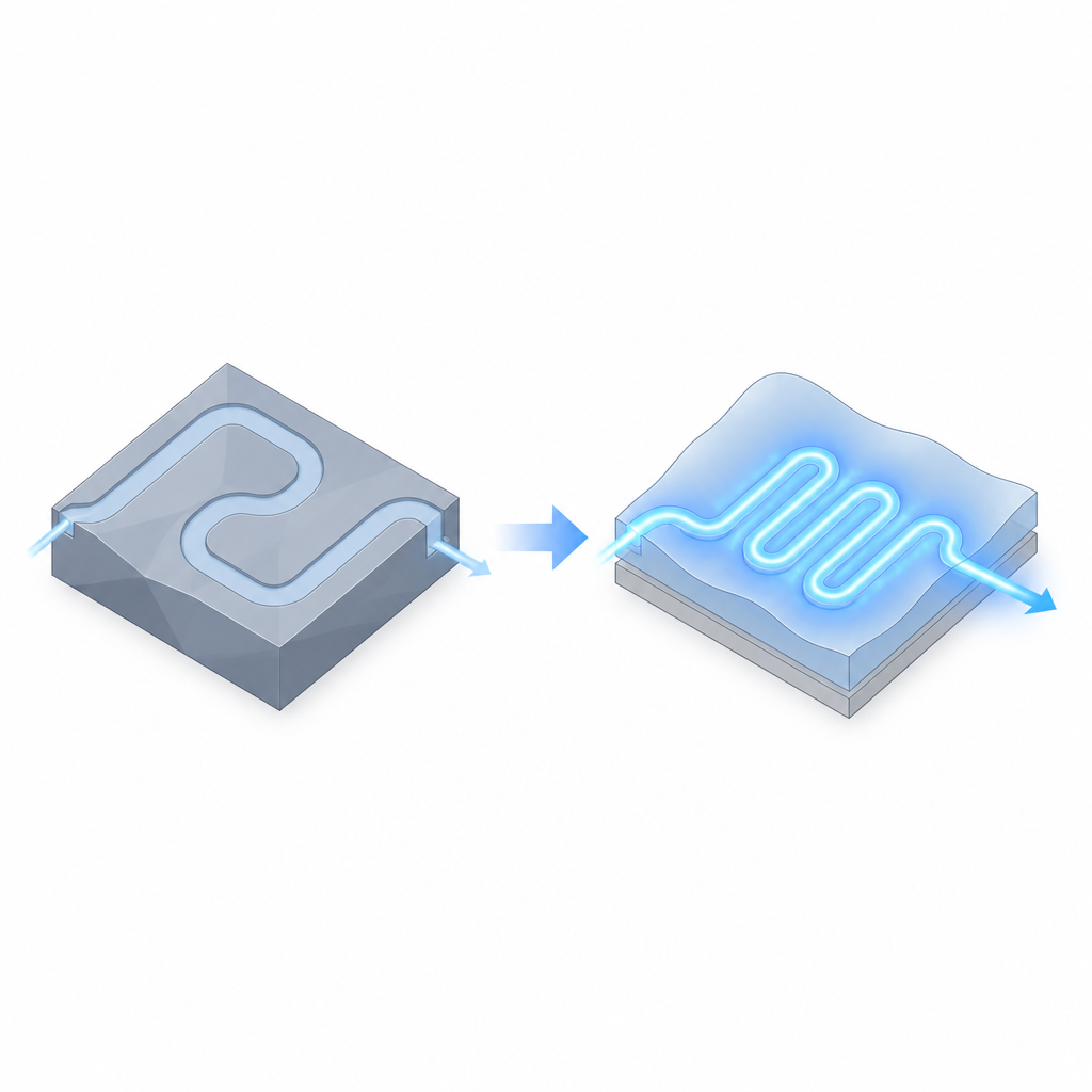
Carving waveguides and checking what survives
Next, the authors turn these activated films into true light guiding structures. They use standard ultraviolet lithography and plasma etching to cut narrow channels in the poled layer, forming waveguides that sit on a glass substrate. Crucially, they place the channels so that they overlap with the bright bands observed earlier. Microscopy images taken after etching show that the special light mixing signal remains concentrated exactly where the waveguides run, even when the surrounding film has been completely removed. In some designs, both horizontal and vertical directions of this response are preserved and can be separately visualized, confirming that the fine geometric pattern written during poling survives the harsh fabrication steps.
Finding the sweet spot for stronger signals
To make the most efficient devices, the waveguides must sit at just the right distance from the original electrode edges. The team systematically shifts the position of the etched channels and repeats the light mapping. They observe that the strongest response in the completed waveguides matches the peak seen in the poled film before etching, at a lateral offset of about seven micrometers from the electrode center. This close agreement shows that the earlier maps can be used as a reliable guide when designing lithography masks, and that the internal rearrangement of charges in the glass is not disturbed by patterning, heating, or storage over more than a year.
What this means for future light based chips
In simple terms, the study shows that strong, long lasting light mixing regions can be written into a glass like niobium oxide film, and that these regions remain intact after the film is sculpted into waveguides using standard chip fabrication methods. By aligning the etched channels with the mapped active zones, engineers can build compact devices that harness second order optical effects without relying on hard to process crystals. This approach could support a new generation of integrated components, such as electro optic modulators and chip scale spectrometers, built on versatile amorphous films that are easier to manufacture and integrate with other photonic platforms.
Citation: Boonsit, S., Karam, L., Adamietz, F. et al. Sustained poling-induced second-order optical nonlinearity in sodium-doped amorphous niobium oxide waveguides. Sci Rep 16, 15146 (2026). https://doi.org/10.1038/s41598-026-45779-5
Keywords: nonlinear optics, waveguides, lithium niobate, amorphous thin films, integrated photonics