Clear Sky Science · en
Geo-spatial prospective life cycle sustainability of InGaN and InGaP compound semiconductors
Why the Future of Tiny Lights Matters
From phone screens to virtual reality headsets, ever-smaller and brighter light-emitting diodes (LEDs) are shaping how we see and interact with the digital world. Two advanced materials, InGaN and InGaP, are front-runners for next‑generation micro‑LED displays, but they come with hidden environmental and resource costs. This study asks a simple but crucial question: if we are going to build billions of these devices, where in the world should we make them, and how, so that we minimise harm to the planet over the coming decades?
Following a Chip Around the World
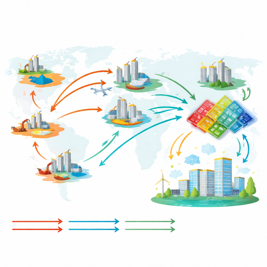
The researchers map out the full journey of these compound semiconductors, from raw minerals in the ground to finished devices ready to light up screens. They examine 80 different global supply chain configurations for InGaN and InGaP, involving 11 countries and four key stages: extracting indium, gallium and phosphorus; fabricating wafers in specialised cleanrooms; testing and packaging the devices; and finally shipping them to major electronics markets. By combining this geographic detail with life cycle assessment, they calculate 18 kinds of environmental impact for each configuration, including climate warming, water use, toxic pollution and depletion of scarce minerals, for the years 2024, 2030, 2040 and 2050.
How Cleaner Power Changes the Picture
A central finding is that electricity dominates the environmental footprint of these chips, especially during energy‑hungry steps such as epitaxial growth (where ultra‑thin crystal layers are deposited) and maintaining ultra‑clean rooms. As many countries shift their power grids away from coal and gas toward renewables, the impacts of making InGaN and InGaP devices drop sharply. For example, one scenario with fabrication in Taiwan shows the climate impact of InGaN production falling by about three‑quarters between 2024 and 2050. Across almost all scenarios, impacts converge to much lower levels by mid‑century, reflecting global decarbonisation—yet important differences between countries remain.
Why Location Still Matters
Even in 2050, where you fabricate these semiconductors strongly affects how sustainable they are. Supply chains that place the most energy‑intensive steps in regions with cleaner electricity and stronger pollution controls—such as the UK and USA, and increasingly Taiwan—consistently score best across climate, toxicity and resource‑use indicators. By contrast, scenarios that concentrate mining, fabrication, testing and use in coal‑reliant regions, particularly China, show the highest impacts for global warming, air and water pollution and water depletion. The study also shows that simply shortening transport routes or keeping everything in one country does not guarantee lower impacts; the local power mix and environmental regulations matter far more than shipping distances.
Inside the Factory: Shifting Hotspots
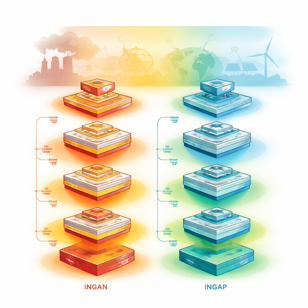
As electricity grids become cleaner, the environmental “hotspots” within the manufacturing process shift. Today, the cleanroom’s constant air filtration and cooling are major contributors. Over time, as their electricity becomes greener, the relative importance of material and chemistry‑intensive steps grows. Epitaxial growth, substrate preparation, photolithography and metal deposition become the main sources of climate, toxicity and water impacts, particularly for InGaP. The choice of substrate and gases matters: InGaP, grown on gallium arsenide and using more complex chemistries, tends to drive higher marine and human toxicity and greater pressure on mineral resources than InGaN, which uses simpler inputs. However, InGaP has an advantage in stratospheric ozone depletion because it relies less on halogen‑containing chemicals.
Choosing the Better Path for Tiny LEDs
For non‑specialists, the take‑home message is that advanced LEDs are not automatically “green” just because they are efficient when operating. Their true footprint depends on where and how they are made, and on the materials and chemicals that go into them. This study shows that placing key fabrication steps in regions with cleaner power and stricter environmental rules, redesigning processes to reduce reliance on hazardous gases and scarce minerals, and improving recycling of indium and gallium can greatly cut the harm from future micro‑LED production. Overall, InGaN usually comes out as the less damaging option, but the best outcomes combine careful material choice with smart, geographically aware supply‑chain design.
Citation: Shamoushaki, M., Travers-Nabialek, J., Gillgrass, SJ. et al. Geo-spatial prospective life cycle sustainability of InGaN and InGaP compound semiconductors. Sci Rep 16, 13659 (2026). https://doi.org/10.1038/s41598-026-43622-5
Keywords: compound semiconductors, micro-LEDs, life cycle assessment, semiconductor supply chains, sustainable manufacturing