Clear Sky Science · en
Dielectric function of layered GaSe0.8Te0.2 and emergent all van der Waals optical elements
Why ultrathin light tools matter
From smartphone sensors to quantum communication, modern technologies increasingly rely on devices that can steer and shape light on a chip. To shrink these optical components down while keeping them efficient, researchers need materials that bend light strongly without absorbing it. This study explores a new member of the two-dimensional crystal family—a layered compound called GaSe0.8Te0.2—and shows that it can serve as a powerful building block for ultrathin, fully layered optical elements such as beam splitters.
A new layered crystal for guiding light
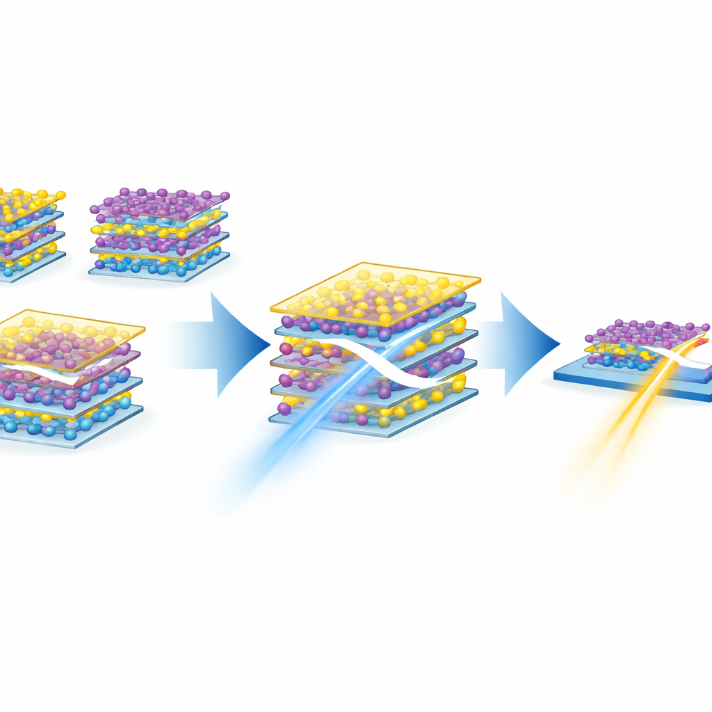
The work focuses on a family of materials known as group III monochalcogenides, which can be peeled into very thin, sheet-like crystals held together by gentle van der Waals forces. By mixing selenium (Se) and tellurium (Te) within gallium-based compounds, scientists can create “ternary alloys” whose properties fall between those of the pure end members. In this study, the authors investigate flakes of GaSexTe1−x with x = 0.8, meaning the crystal is rich in selenium but still contains a significant amount of tellurium. Using optical emission and vibrational fingerprints (photoluminescence and Raman spectroscopy), combined with elemental analysis, they confirm both the internal structure and the Se:Te ratio of the material, showing it adopts a single, orderly hexagonal phase well suited for optical applications.
How strongly the crystal bends and absorbs light
To understand how this crystal handles light, the team measures its dielectric function—the quantity that determines how light propagates through a material—across visible to near-infrared wavelengths (360–1000 nm). They use spectroscopic ellipsometry, a technique that infers optical properties from how the polarization of reflected light changes upon bouncing off the surface. Because the crystal is layered, it responds differently to light traveling within the atomic planes than to light traveling perpendicular to them. The measurements reveal that, in-plane, the material has a very high refractive index, around three at red wavelengths, yet absorbs remarkably little light until the deep-red region where absorption begins. This combination of strong bending and low loss is exactly what is needed for compact, interference-based optical components.
Checking theory against experiment
The researchers go beyond measurement by performing advanced first-principles calculations that predict both the electronic bandgap and the wavelength-dependent optical response of a closely related structural model. These simulations reproduce the shape and magnitude of the experimentally determined refractive indices and absorption, lending confidence that the microscopic description of the material is accurate. They also examine how the in-plane refractive index would change if the Se:Te ratio were varied across different compositions. The results show a practical “tuning window” between the responses of pure GaSe and GaTe, indicating that engineers could dial in desired optical properties simply by adjusting composition within the GaSe–GaTe family.
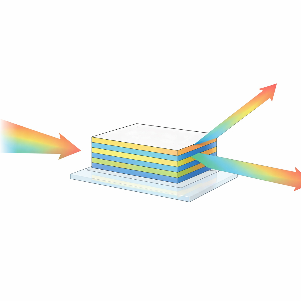
Building all-layered beam splitters
Armed with precise optical constants, the authors design ultrathin beam splitters made entirely from van der Waals materials. They combine high-index GaSe0.8Te0.2 with a low-index layered material, hexagonal boron nitride (hBN), stacking a few alternating sheets on a transparent substrate. By carefully choosing layer thicknesses, they exploit interference—multiple reflections inside the stack—to split an incoming, unpolarized light beam into reflected and transmitted parts with prescribed ratios such as 50:50, 30:70, or 10:90 in the near-infrared range widely used in photonics and lasers. Importantly, they achieve these functions with sub-micron total thickness and only a handful of layers, far fewer than traditional oxide or metal-dielectric coatings require.
From tailored crystals to future light chips
The study shows that GaSe0.8Te0.2 is a rare combination: a strongly light-bending, weakly absorbing, directionally anisotropic crystal that can be stacked with other van der Waals materials to form entirely layered optical devices. By mapping its dielectric function in detail and demonstrating realistic designs—and even a prototype—for beam splitters, the authors provide both the raw data and the design rules needed for practical integration. More broadly, their calculations point to a route for creating a whole family of “designer” light-guiding materials by adjusting alloy composition, paving the way for compact, tunable, chip-scale optical elements built from stacks of two-dimensional crystals.
Citation: Margaryan, A.V., Sargsyan, M.L., Piyanzina, I.I. et al. Dielectric function of layered GaSe0.8Te0.2 and emergent all van der Waals optical elements. Sci Rep 16, 12551 (2026). https://doi.org/10.1038/s41598-026-42182-y
Keywords: van der Waals photonics, high index 2D materials, GaSeTe alloys, ultrathin beam splitters, optical dispersion tuning