Clear Sky Science · en
Contact engineering of metallic Ni-integrated niobium sulfide via H2S treatment for enhanced MoS2 transistor performance and CMOS compatibility
New Building Blocks for Future Computer Chips
As our devices shrink and grow more powerful, the traditional material of choice—silicon—is reaching its physical limits. This study explores a clever way to wire up a new class of atomically thin materials so that they can work reliably inside future computer chips. By redesigning the tiny metal contacts that feed current into these ultra-thin layers, the researchers show how to build faster, more heat-resistant transistors that could keep electronics shrinking for years to come.
Why Ultra-Thin Materials Need Better Connections
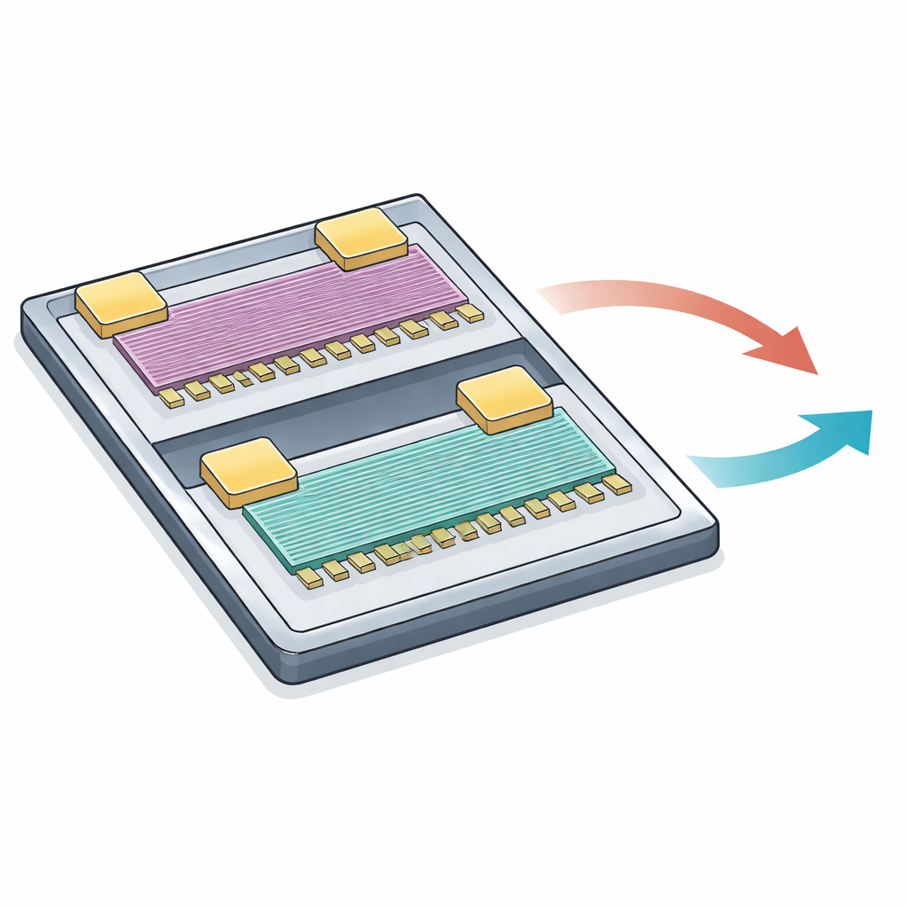
Modern transistors work by steering electric current through a channel. In today’s chips, that channel is usually silicon, but when silicon is shaved down to just a few atoms thick, its performance drops sharply. In contrast, atomically thin crystals called transition metal dichalcogenides (TMDCs), such as molybdenum disulfide (MoS2) and tungsten diselenide (WSe2), can keep their high performance even at these extreme thicknesses. A major obstacle, however, is how to connect metal wires to these fragile layers without creating a lot of resistance at the interface, which wastes energy and slows devices down. Conventional metals tend to react with or disturb the TMDC, so engineers are searching for metal layers that can rest on top like sheets of paper, making clean, gentle “van der Waals” contacts.
A Tailored Metal Layer for Electron-Carrying Devices
The authors focus on transistors that carry negative charges (electrons), known as n-type field-effect transistors, built with a single layer of MoS2 as the channel. They start from a metallic TMDC called niobium disulfide (NbS2), which naturally has properties suited for the opposite kind of device—p-type transistors that carry positive charges. By inserting a small amount of nickel (Ni) into NbS2 using a heat treatment in hydrogen sulfide gas, they transform its internal structure and electronic behavior, creating a new compound written as Ni0.19Nb1.16S2. This new metal layer forms a clean, sheet-like contact on top of monolayer MoS2, allowing electrons to flow into the channel much more easily. Devices using this contact show significantly higher current in the “on” state than devices using either pure NbS2 or pure nickel.
How the New Contact Forms Without Damaging the Channel
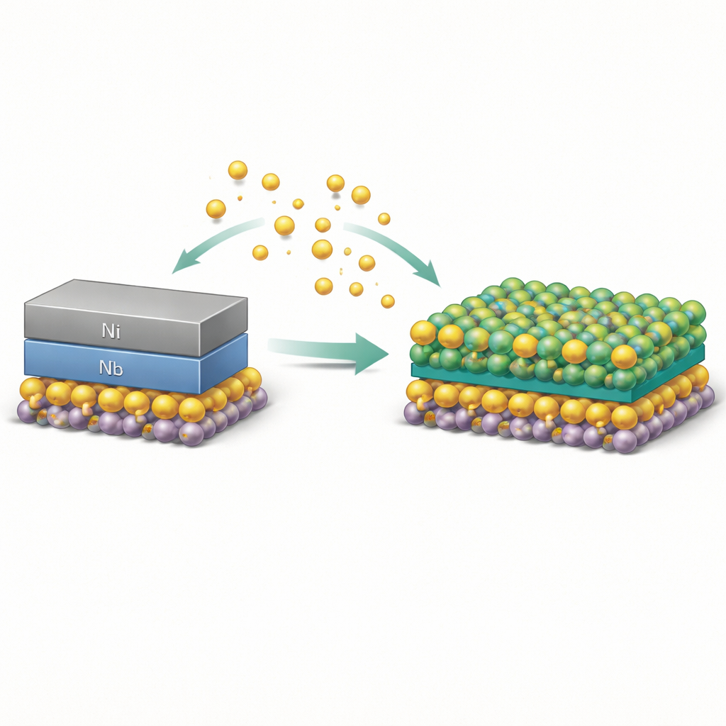
To understand what happens during the heat treatment, the researchers carefully examined cross-sections of the layers with advanced electron microscopes. They first stacked an ultrathin nickel film on MoS2, then added a thin niobium film on top, and finally exposed the stack to hot hydrogen sulfide gas. Under these conditions, sulfur reacts with niobium and nickel to form a layered metal sulfide. Microscopy and elemental mapping reveal that the resulting Ni0.19Nb1.16S2 forms a well-ordered crystal sitting directly on MoS2 with a van der Waals interface, and—crucially—neither nickel nor niobium diffuse into the MoS2 layer. When they tried similar heat treatments with nickel alone or niobium alone, those metals did diffuse into the MoS2 and mixed with it, which would degrade transistor performance. The combination stack, in contrast, naturally rearranges into a stable layered metal that preserves the integrity of the underlying atomic sheet.
Balancing Composition for Best Performance and Heat Resistance
The team systematically varied the thicknesses of the starting nickel and niobium layers to tune the final contact. They found that the amount of niobium largely sets the thickness of the resulting Ni0.19Nb1.16S2 layer, while excess nickel tends to gather on the surface. Electrical tests on many devices showed that a particular combination—roughly one nanometer of niobium on an ultrathin nickel layer—produced contacts with the best balance of high current and reproducibility. Measurements over a range of temperatures indicated that the energy barrier for electrons to cross from the contact into the MoS2 channel is very low, close to that of pure nickel contacts but without nickel’s tendency to intermix with MoS2. When the researchers heated devices with ordinary nickel contacts to 600 °C, their performance dropped sharply, whereas devices with Ni0.19Nb1.16S2 contacts maintained both strong current and high electron mobility, demonstrating superior thermal robustness.
Toward Complete Circuits with Atomically Thin Materials
For a full logic circuit, chipmakers need both n-type and p-type transistors, a combination known as CMOS. Previous work showed that pure NbS2 metal is well suited as a contact for WSe2-based p-type devices, but its properties make it a poor choice for MoS2 n-type devices. This study reveals that by carefully adding nickel and using the same hydrogen sulfide heat treatment, NbS2 can be converted into Ni0.19Nb1.16S2, which is ideal for n-type MoS2 devices. In other words, a single industrially compatible process can create two different, tailored contacts—NbS2 for p-type and Ni0.19Nb1.16S2 for n-type—each matched to a different atomically thin channel. For non-specialists, the take-home message is that the authors have found a way to “rewire” a promising metallic material so that it provides clean, low-resistance, and heat-tolerant connections to next-generation ultra-thin transistors, bringing fully two-dimensional CMOS technology a practical step closer.
Citation: Hori, K., Chang, W.H., Irisawa, T. et al. Contact engineering of metallic Ni-integrated niobium sulfide via H2S treatment for enhanced MoS2 transistor performance and CMOS compatibility. Sci Rep 16, 12591 (2026). https://doi.org/10.1038/s41598-026-41610-3
Keywords: 2D transistors, MoS2, contact engineering, CMOS, van der Waals contacts