Clear Sky Science · en
Design and simulation of a p-type dual interbridge treeFET with comprehensive DC, analog/RF, and linearity analysis for CMOS circuit applications
Smaller, Faster Chips for Everyday Tech
From smartphones to Wi‑Fi routers, modern gadgets rely on billions of microscopic switches called transistors. Engineers keep shrinking these switches to pack more power into smaller chips, but today’s designs are running into physical limits: they leak current, waste energy, and distort high‑frequency signals. This paper explores a new kind of transistor, shaped like a tiny three‑dimensional tree, that could help keep performance climbing for future low‑power, high‑speed electronics.
A New Tree‑Like Transistor Shape
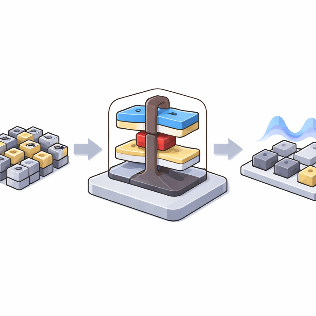
The device studied here is called a p‑type Dual Interbridge TreeFET, a switch built for technology generations smaller than three billionths of a meter. Instead of a simple flat channel, it uses two thin, flat “nanosheets” stacked on top of each other, connected by two vertical bridges in a tree‑like form. This three‑dimensional structure lets current flow through several paths at once while the surrounding gate metal keeps tight control over the charge inside. That combination increases the useful current when the transistor is on and cuts down on unwanted current when it is off, all within an extremely small footprint suited to dense logic chips.
Tuning the Space Around the Switch
A key idea in this work is that not only the core of the device matters, but also the thin insulating regions that sit beside the gate, called spacers. The authors used detailed computer simulations to compare different spacer materials, from empty space (air) to common oxides and a “high‑k” material called hafnium oxide. High‑k simply means the material responds strongly to electric fields. When hafnium oxide was used beside the gate, the electric field wrapped the channel more effectively, making it easier for holes (the charge carriers in this p‑type device) to move when the transistor is on, while still keeping the barrier high enough to block them when it is off.
Balancing Power, Leakage, and Signal Quality
The study shows that with hafnium oxide spacers the tree‑like transistor delivers close to 40 percent more on‑current, sharper switching between off and on, and much better resistance to short‑channel effects that usually plague very small devices. These gains come from stronger electrostatic grip of the gate over the channel and an increase in gate capacitance, which improves how effectively the device responds to input voltage. However, there is a trade‑off: while high‑k spacers boost raw drive strength, they also increase certain parasitic capacitances that can limit the ultimate radio‑frequency speed and worsen some subtle nonlinear behaviors that cause signal distortion in sensitive analog and wireless circuits. In contrast, simpler low‑k spacers like air produce cleaner, more linear responses and higher cut‑off frequencies, but with lower drive current.
From Single Device to Working Circuit
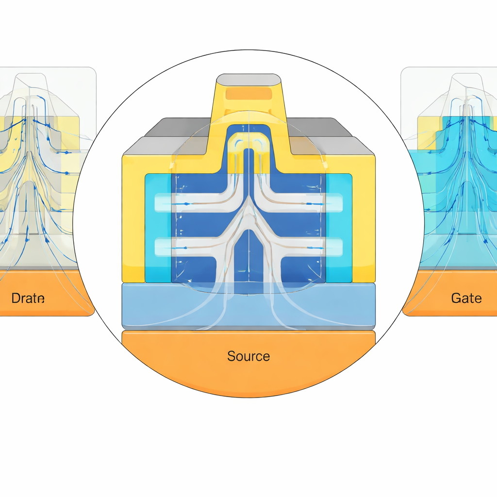
To show that this design is not just a theoretical curiosity, the authors built a simulated three‑stage voltage‑controlled oscillator using both n‑type and p‑type versions of the TreeFET. This kind of circuit is a key building block in radios, clocks, and communication links because it generates a tunable periodic signal. In the simulations, the oscillator reached frequencies above 20 gigahertz while running at a modest supply voltage, and its frequency could be smoothly adjusted by changing a control voltage. The strong gate control and compact geometry of the TreeFET helped keep the oscillations stable while offering a wide tuning range that is attractive for future wireless and mixed‑signal chips.
What This Means for Future Electronics
For a non‑specialist, the main message is that the authors have identified a realistic way to keep shrinking the basic transistor while still improving its behavior for both digital and high‑frequency uses. By carefully engineering the three‑dimensional tree‑like channel and the spacer materials that surround it, they show how to trade between maximum drive strength and the cleanliness of analog signals. High‑k spacers favor strong, energy‑efficient switching for logic circuits, while low‑k spacers offer cleaner, less distorted signals for radio‑frequency blocks. This flexibility suggests that Dual Interbridge TreeFETs could become versatile building blocks for future system‑on‑chip designs that demand high speed, low power, and reliable wireless communication in ever smaller devices.
Citation: Mounika, S., Nanda, U. Design and simulation of a p-type dual interbridge treeFET with comprehensive DC, analog/RF, and linearity analysis for CMOS circuit applications. Sci Rep 16, 11144 (2026). https://doi.org/10.1038/s41598-026-41484-5
Keywords: nanosheet transistor, advanced CMOS, RF circuits, device scaling, voltage controlled oscillator