Clear Sky Science · en
Optimization of enhancement-mode MIS-GaN HEMT with dual channel for simple process using TCAD simulation
Why smarter power switches matter
Modern gadgets, electric cars, and fast chargers all rely on electronic switches that turn power on and off millions of times per second. Gallium nitride (GaN) devices are emerging as the next generation of these switches because they can handle high voltages and work very efficiently. However, many GaN switches are naturally “on” unless a special control voltage forces them off, which complicates circuits and can be unsafe. This paper explores a new GaN transistor design that naturally stays off while still being relatively simple to manufacture.
Two layers instead of one
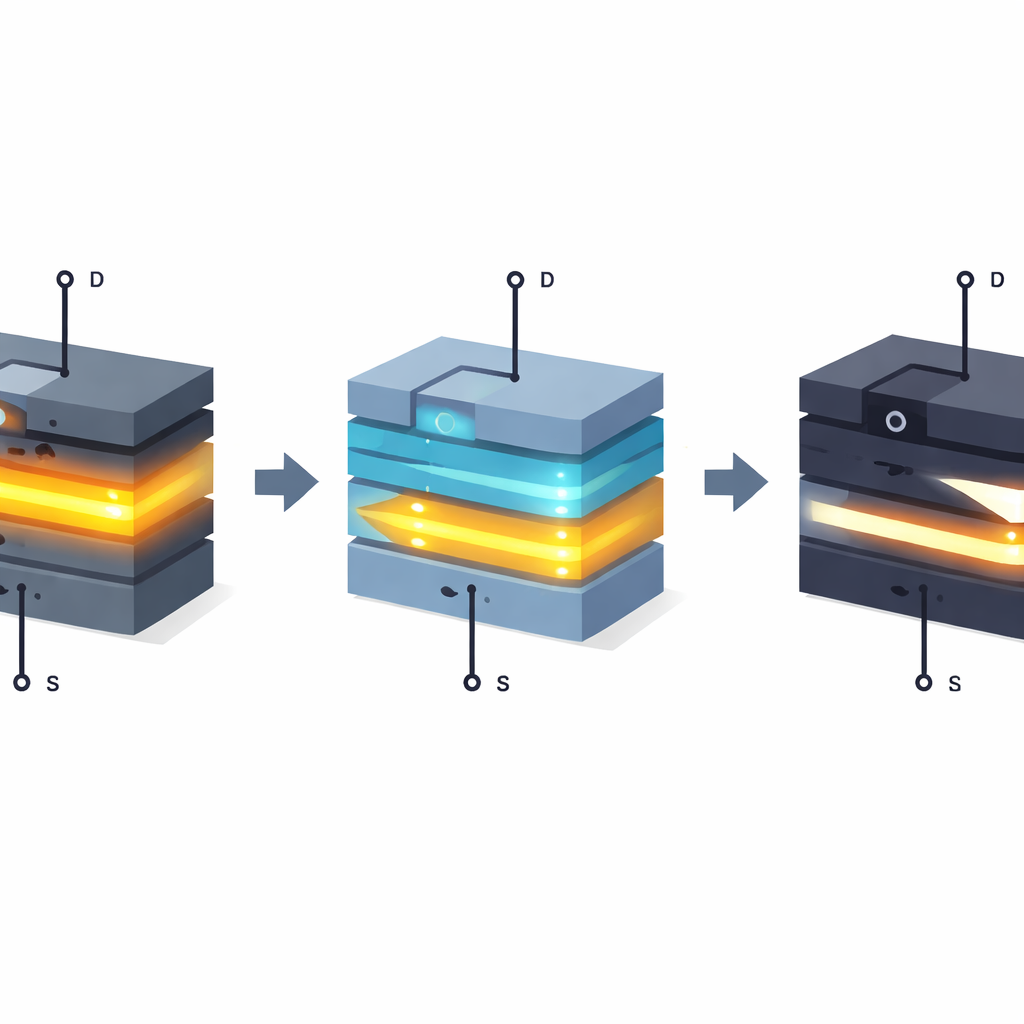
The researchers focus on a type of GaN device called a high electron mobility transistor, or HEMT, which normally uses a single ultra-thin layer where electrons move very quickly. In the conventional version, this layer forms a highly conductive path as soon as the device is made, so the transistor is in a default “on” state. The team proposes adding a second, buried conducting layer beneath the usual one, creating a “dual-channel” structure. Crucially, only the upper layer is used to carry current between the source and drain; the lower layer is deliberately kept out of the main current path and is instead used as an internal control element.
How the hidden layer tilts the balance
Using detailed computer simulations calibrated against a real, single-layer device, the authors show how the buried layer acts like a built-in negative voltage source. Because it is filled with electrons, this lower layer behaves as if it were holding a permanent negative charge underneath the active channel. That negative charge subtly pulls up the energy landscape of the upper layer, making it harder for electrons to gather there. As a result, the transistor no longer conducts at zero gate voltage: a positive control voltage is now required to pull electrons back into the upper layer and create a continuous path for current. This shift in behavior turns a normally-on switch into a normally-off one.
Balancing safety and performance
The study compares the new dual-channel device with a traditional single-channel version that was actually fabricated and measured. When translated into everyday terms, the results show a trade-off: the new design raises the “turn-on” point of the device by about 1.7 volts, successfully making it normally off, but it also slightly worsens how easily current can flow when it is on. This is because the adjustments that help push the device into the off state—such as thinning one of the key layers and lowering its aluminum content—also reduce the number of electrons available in the main path. The simulations further reveal that the dual-channel structure modestly lowers the voltage at which the device breaks down under stress, due to how charges build up between the two channels.

Tuning the layers like knobs
One of the strengths of the proposed design is that it offers several “knobs” engineers can turn to fine-tune behavior. By adjusting the thickness and composition of the two barrier layers that form the channels, the team shows they can move the turn-on voltage in a controlled way, at the cost of some current capability. They also demonstrate that making the insulating layer under the gate thinner allows the gate to more effectively pinch off the channel, pushing the turn-on voltage as high as about 1.3 volts while maintaining stable normally-off operation. This tunability suggests the structure could be adapted to different power applications with varying safety margins and efficiency targets.
What this means for future electronics
For non-specialists, the key takeaway is that the authors have devised a clever way to hide a kind of built-in “brake” inside a GaN transistor, using an extra buried channel that is never meant to carry the main current. This internal brake shifts the device from a default on state to a default off state without relying on complex and delicate processing steps that are hard to control in mass production. Although the new design sacrifices some raw performance and breakdown strength compared with the best conventional devices, it offers a simpler path to safer, normally-off GaN switches. That combination of safety, simplicity, and adjustability could make it attractive for future high-efficiency power converters and other demanding electronic systems.
Citation: Lee, K.H., Yang, Y., Heo, J. et al. Optimization of enhancement-mode MIS-GaN HEMT with dual channel for simple process using TCAD simulation. Sci Rep 16, 11068 (2026). https://doi.org/10.1038/s41598-026-41105-1
Keywords: gallium nitride power transistor, normally off GaN HEMT, dual channel device, power electronics switches, TCAD device simulation