Clear Sky Science · en
DNN-assisted waveguide width extraction via optical measurement of a single low-order Mach-Zehnder interferometer
Why measuring tiny light paths matters
Inside the data centers and future quantum computers that move information with light instead of electricity, hair‑thin glasslike tracks called waveguides steer that light around a chip. The exact width of these tracks turns out to be crucial: change it by just a few billionths of a meter and the behavior of the light can shift enough to hurt speed, power use, or signal quality. Yet checking those dimensions usually means cutting open chips and peering at them with expensive microscopes. This study introduces a faster, non‑destructive way to “read out” waveguide width using only a simple optical test structure and a deep‑learning model.
Light as a ruler on a chip
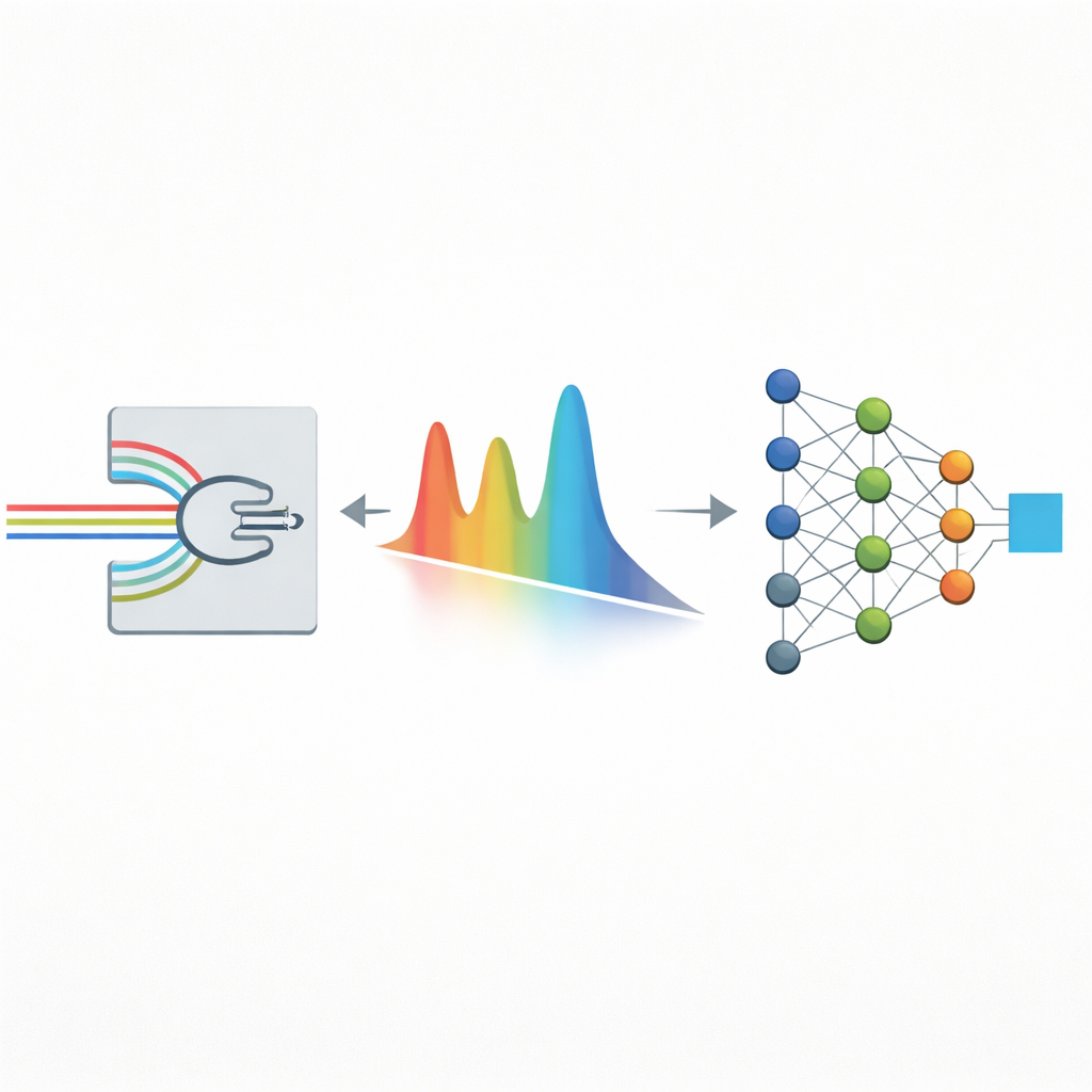
The authors build on a classic device from optics called a Mach–Zehnder interferometer, which splits a beam of light into two paths and then recombines them. If one path is even slightly different from the other, the outgoing light forms a distinctive pattern of bright and dark fringes across different colors, much like the ripples you see when two sets of waves meet on water. Because this pattern is sensitive to how tightly light is confined in a waveguide, it indirectly encodes information about the waveguide’s width. The team designs a particularly compact version of this interferometer on a silicon photonics platform, with the two arms identical except for a very small length difference of only 26.672 micrometers—far shorter than the structures typically used for such measurements.
Turning complex spectra into simple dimensions
Rather than relying on traditional curve‑fitting formulas, which struggle when the physics becomes strongly nonlinear, the researchers turn to a deep neural network. They first use computer simulations to show how the effective optical properties of the waveguide change with both wavelength and width over realistic fabrication ranges. From these simulations they generate a large set of example spectra paired with their true widths and use this database to train a fully connected neural network to act as an inverse model: given the optical behavior, it predicts the physical width. The trained model reaches an impressive mean absolute error of just 0.15 nanometers on unseen simulated data, indicating that it has captured the intricate relationship between spectrum and geometry far beyond what simple polynomials can easily express.
From lab measurements to real devices
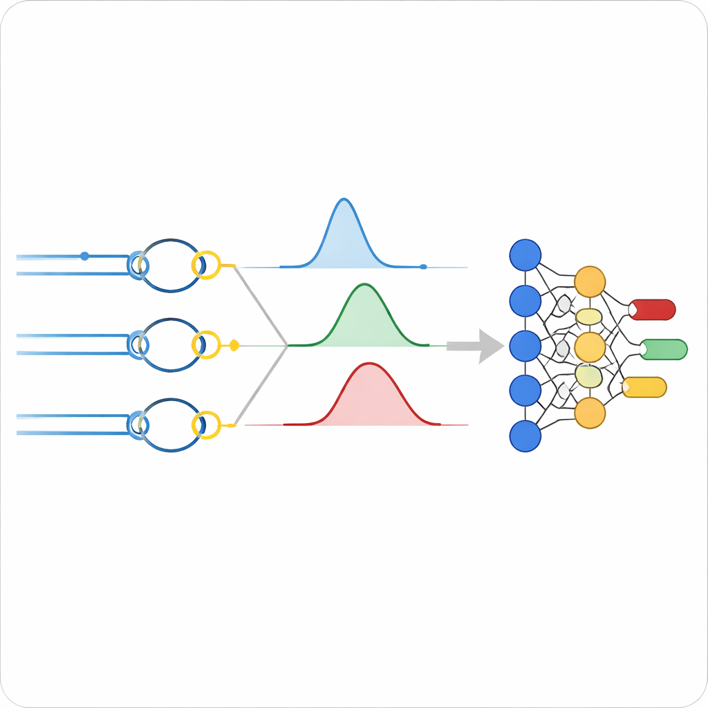
To test the method in practice, the team fabricates 30 interferometer devices on a standard silicon‑on‑insulator wafer, with actual waveguide widths spread across a ±20‑nanometer range around the design value. They shine a tunable laser through each tiny structure and record the transmitted spectrum in the telecommunications C‑band. By carefully locating specific dark troughs in the pattern and estimating how closely spaced these troughs are, they determine a pair of optical quantities—effective index and group index—that together identify which fringe order they are observing. These values are then fed into the pre‑trained neural network, which returns a predicted physical width for each device, all without cutting into the chip.
How close it comes to a microscope
The authors then compare these optical predictions against direct measurements made with a scanning electron microscope, which serves as the gold standard. Across the 30 devices, the new method achieves an average error of only 3.28 nanometers, with the worst case still below 6.7 nanometers. The study further analyzes where the remaining discrepancies come from, tracing them to routine uncertainties in spectral measurements, slight variations in the angle of the waveguide sidewalls, and tiny changes in layer thickness that were not included in the training simulations. Even accounting for these real‑world imperfections, the approach proves robust and accurate enough for monitoring how well a fabrication process is holding its target dimensions.
Smaller test structures, smarter control
By combining a single, very compact interferometer with a deep‑learning model trained on realistic simulations, this work shows that chip makers can quickly and non‑destructively read out waveguide widths with nearly microscope‑level precision. That means they can spot drifts in lithography or etching steps within minutes of a wafer leaving the line, instead of waiting for off‑line imaging. The same strategy could be expanded to track several geometric parameters at once, simply by enriching the training data and adding more optical features. In the longer term, such AI‑assisted metrology may become a key feedback tool for building denser, more reliable photonic circuits that carry the world’s data on beams of light.
Citation: Wang, F., You, H., Xu, X. et al. DNN-assisted waveguide width extraction via optical measurement of a single low-order Mach-Zehnder interferometer. Sci Rep 16, 12260 (2026). https://doi.org/10.1038/s41598-026-41085-2
Keywords: silicon photonics, waveguide metrology, Mach-Zehnder interferometer, deep neural networks, optical characterization