Clear Sky Science · en
Effect of metasurface and process parameters on adhesion during transfer printing using a nanoscratch test
Why tiny patterns matter for giant screens
Ultra-sharp 4K and 8K images are pushing display technology to its limits. To pack more pixels into the same space, engineers are turning to "metasurfaces"—ultra-thin metallic structures that can finely steer light. But making and moving these delicate patterns from a production mold onto a working screen is tricky: if they stick too strongly to the mold or not strongly enough to the screen, the transfer fails. This study digs into how and why these tiny structures stick or peel, and shows how to tune pressure and temperature so metasurfaces can be reliably printed for next-generation displays.
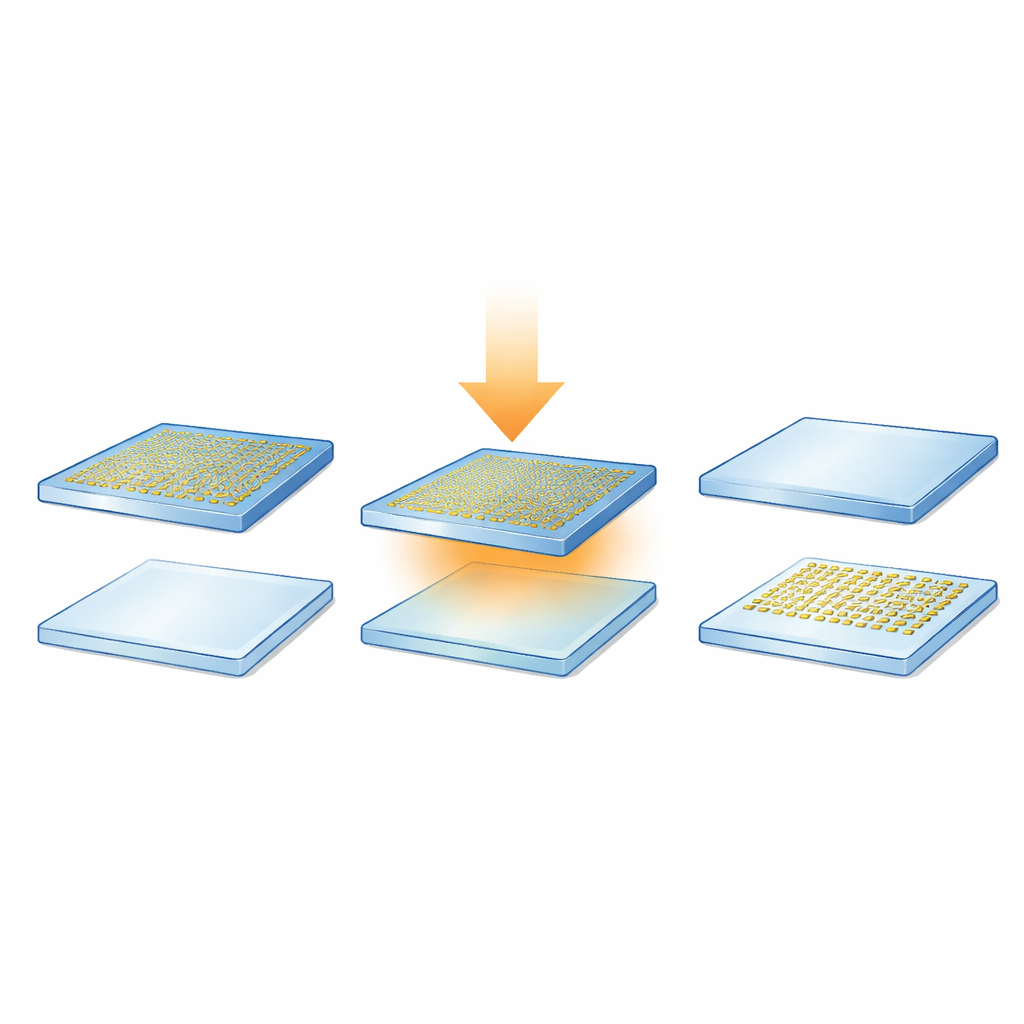
From factory mold to working display
In transfer printing, a thin metallic layer patterned into a metasurface is first formed on a reusable mold and then moved onto a separate substrate that will become part of the display. The key is adhesion: the metasurface must let go of the mold while gripping the new substrate more strongly. Too much grip on the mold and the pattern will not transfer; too little grip on the substrate and it will later peel off, ruining the pixel. The authors built a controlled model of this process using silver-based metasurfaces and silicon supports, creating four versions of molds and four matching substrates that mimicked real manufacturing conditions.
Scratching at the nanoscale to measure stickiness
Measuring how firmly layers stick together is surprisingly hard when those layers are only a few hundred nanometers thick. Common industrial tests work on millimeter scales and cannot resolve what happens inside a single pixel. Instead, the team used a nanoscratch test: a diamond tip presses down with a controlled force and is dragged laterally across the surface. As the scratch progresses, the thin metallic film eventually buckles and peels. By matching scanning electron microscope images of where peeling begins with the recorded forces at that exact point, the researchers could convert a scratch track into a precise measure of adhesion at the buried interface.
How surface shape, pressure, and heat change the grip
The metasurface itself changes the contact in subtle ways. On the mold side, its tiny holes cause both helpful and harmful effects: filling the holes allows the metal to mechanically lock into the mold, but the same geometry also creates small dimples that shorten the path for cracks to grow, making peeling easier. These opposing effects nearly cancel, so the mold’s adhesion changes only slightly when the metasurface is present. On the substrate side, however, the story is different. When the dimpled metal is pressed onto a flat, treated silicon surface, it leaves voids—tiny gaps where there is no contact at all. This drastically reduces the real contact area and cuts the measured adhesion by about 85 percent compared with a flat metal layer.
Finding the sweet spot of pressure and temperature
To counter this loss of contact, the team raised the pressure during transfer from 1 bar (roughly room conditions) to 5 bar. Higher pressure squeezed the metal into both mold and substrate, strengthening mechanical interlocking and shrinking the voids. On the substrate side, adhesion became so strong that the rigid silicon support fractured before the metasurface could peel—evidence that the interface was now tougher than the underlying material. Heating to 90 °C had opposite effects on the two sides. In the mold, heating introduced internal stresses because the polymer base and metal expanded differently, weakening the interface. On the substrate, heat boosted chemical bonding at the treated surface but also increased residual stress; these two influences largely balanced, leaving adhesion similar to the cooler case.
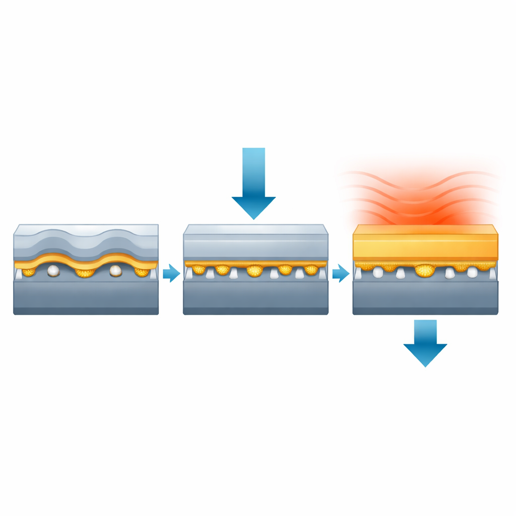
How this guides future ultra-sharp displays
By comparing molds and substrates prepared under matching conditions, the authors showed that reliable transfer requires the substrate to hold the metasurface far more strongly than the mold. Their data reveal that applying 5 bar of pressure at 90 °C delivers the best balance: the mold’s grip is weakened by thermal stress, while the substrate interface becomes extremely robust. In practical terms, this recipe provides a clear, quantitative guideline for manufacturers seeking to mass-produce metasurface-based OLED displays with pixel densities far beyond today’s limits, bringing smoother, sharper images a step closer to everyday devices.
Citation: Park, Y., Choi, DG., Jung, JY. et al. Effect of metasurface and process parameters on adhesion during transfer printing using a nanoscratch test. Sci Rep 16, 12924 (2026). https://doi.org/10.1038/s41598-026-40867-y
Keywords: metasurface, transfer printing, adhesion, ultra-high-resolution displays, nanoscratch testing