Clear Sky Science · en
Magnetic flux imaging in a 3D superconductor integrated circuit
Why Hidden Magnetic Patterns Matter
As computers push toward faster speeds and lower power, engineers are turning to superconducting circuits—chips that carry electrical signals with virtually no resistance. But these delicate circuits can be disturbed by tiny magnetic fields, including Earth’s own magnetism. This paper explores how magnetic flux actually threads its way through a real, eight-layer superconducting logic chip, revealing invisible patterns that can either protect the circuit or quietly undermine it.
A Layered Superconducting City
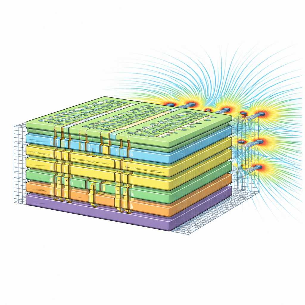
The device under study is a complex digital shift register: thousands of repeating logic cells built from Josephson junctions and superconducting wires, spread across eight ultrathin niobium layers. These active layers are sandwiched between broad “ground planes” of superconducting metal, which help stabilize signals, and surrounded by a fine grid of narrow wires that act as a magnetic shield. The entire chip is only a few millimeters across, yet it contains moats, bridges, and tiny squares of metal fill that together form a three-dimensional maze for magnetic fields.
Taking Pictures of Invisible Fields
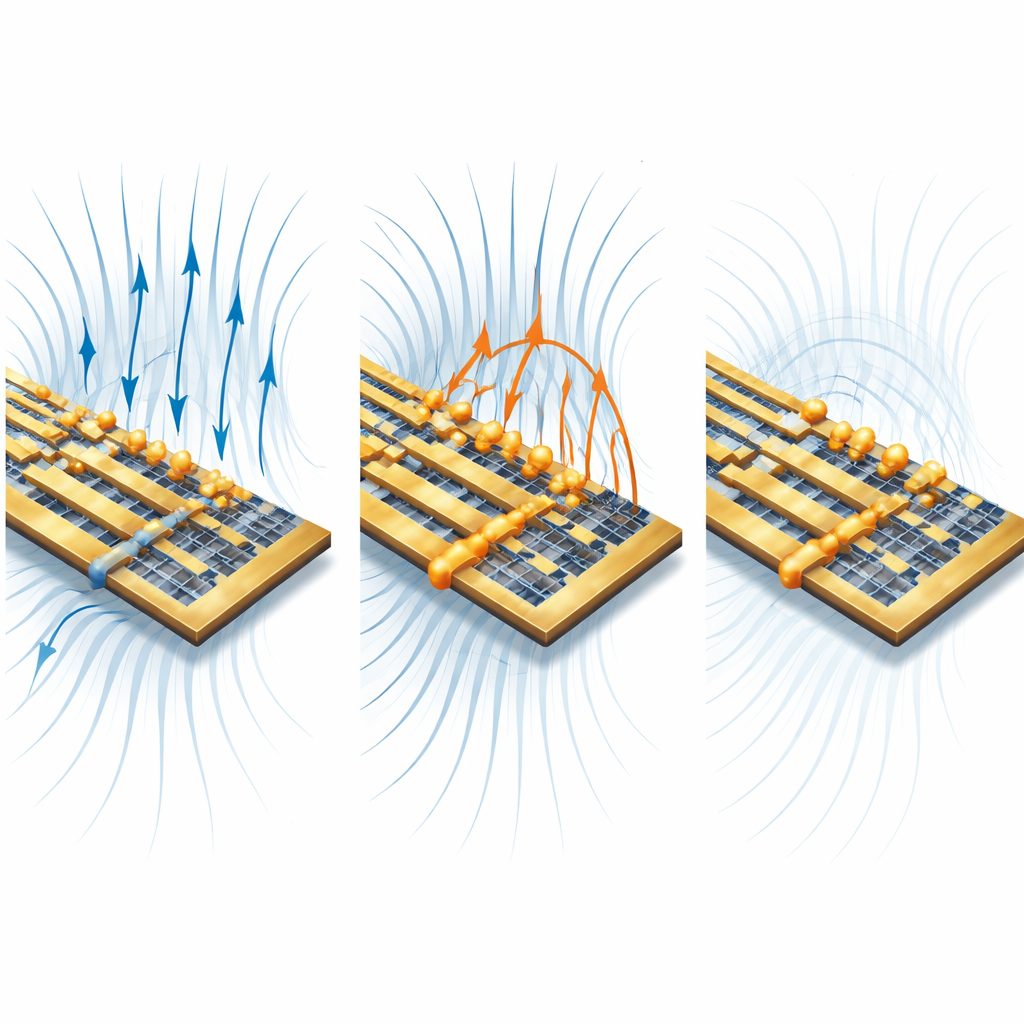
To see how magnetic flux enters this maze, the researchers used magneto-optical imaging. They cooled the chip below the superconducting transition temperature and placed a special transparent indicator film on top. When a magnetic field is applied, the film’s optical properties change in proportion to the local field, allowing a camera to record detailed maps of magnetic induction across the chip’s surface. By ramping the field up and down, or cooling the device in a constant field, the team could watch flux creep in from the edges, rush along preferred paths, and become trapped in specific features of the layout.
Guided Pathways and Magnetic Bottlenecks
The images show that magnetic flux does not seep in evenly. First, it piles up around the large contact pads at the chip’s edge and then threads its way through the surrounding wire grid, forming diagonal channels that steer flux toward the main ground planes. Once there, the flux is strongly concentrated in long slit-like openings—moats cut into the ground planes to manage trapped vortices. Some slits run all the way to the strip edge, while others stop short, and this subtle difference creates “fast lanes” where flux races along linked slits, forming bead-like clusters near narrow bridges between them. Tiny square fill structures in deeper layers further modulate the field, carving out regions where vortices prefer to sit and shaping intricate patterns of high and low magnetic density.
Multilayer Pads and Trapped Flux Landscapes
The contact pads, which connect the chip to the outside world, have their own internal structure: some layers are continuous rectangles of superconductor, while others are arrays of parallel strips. As the field increases, flux first avoids these pads, then penetrates into square pockets between the strip projections, producing a repeating checkerboard of concentrated vortices. When the field is reduced, much of the flux remains trapped, especially along the network of strips and in the moats of the ground planes. Even cooling the chip in a tiny background field leaves a faint but organized pattern: flux is pushed away from bulk superconducting regions and stored preferentially in the designed slits and pockets.
Design Lessons for Future Superconducting Chips
Overall, the chip behaves like a slice of “superconducting Swiss cheese,” where currents in the solid regions steer magnetic flux into carefully arranged holes and channels. The study demonstrates that the surrounding wire grid is effective at shielding moderate magnetic fields, but it also shows that moats and closely spaced slits can locally amplify fields and trigger instabilities, creating secondary vortices even in weak environments. By revealing where flux actually goes—and where it gets stuck—these magnetic images provide a blueprint for refining the shapes and placements of ground planes, slits, grids, and fill structures. That knowledge will be crucial for building the next generation of robust, energy-efficient superconducting electronics and components for quantum technologies.
Citation: Ren, T., Glatz, A., Jankó, B. et al. Magnetic flux imaging in a 3D superconductor integrated circuit. Sci Rep 16, 12452 (2026). https://doi.org/10.1038/s41598-026-40711-3
Keywords: superconducting circuits, magnetic flux imaging, Josephson junction logic, flux trapping, superconductor electronics design