Clear Sky Science · en
Ambipolar thin-film transistors and inverter circuits based on mixed-dimensional bilayer heterostructures
Smarter Electronics from Ultra-Thin Building Blocks
Today’s gadgets—from phones to smartwatches—depend on tiny switches called transistors. As engineers push these switches to be smaller and more efficient, they are turning to materials only an atom or two thick. This study shows a new way to combine two such ultra-thin materials so that a single transistor can behave like both types of switch needed for low-power logic, potentially simplifying how future flexible and large-area electronics are made.
Why New Switches Matter
Modern digital circuits rely on pairs of transistors that pass either negative or positive charge, working together much like a see-saw to save power and resist electrical noise. Molybdenum disulfide (MoS₂), a sheet-like crystal just one molecule thick, is a strong candidate for next-generation electronics because it can carry current well and can be grown over large areas. But it naturally prefers to pass only one kind of charge, making it hard to form the complementary pairs that standard logic circuits rely on without resorting to complex, delicate processing steps. Finding a simple way to add the missing behavior without disturbing the MoS₂ is therefore a key challenge.
Combining Two Worlds in One Channel
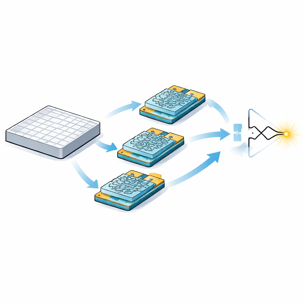
The authors tackle this problem by stacking two very different kinds of materials into a single transistor channel: a flat, two-dimensional MoS₂ layer that favors negative charges, and a random mesh of one-dimensional single-walled carbon nanotubes (SWCNTs) that favor positive charges in air. First, they grow monolayer MoS₂ crystals over large areas using a scalable method and move them onto an insulating layer with a built-in gate electrode underneath. They then use inkjet printing—much like a high-tech desktop printer—to place silver contacts and, later, to deposit a patterned network of nanotubes exactly where they want ambipolar (dual-behavior) devices to sit. This mixed “bilayer” channel lets current flow through either the MoS₂ sheet or the nanotube mesh, depending on how the underlying gate is biased.
One Device, Two Charge Pathways
Before stacking the layers, the team measures individual MoS₂ and nanotube transistors. As expected, MoS₂ conducts when the gate attracts negative charges, while the nanotube devices conduct when the gate attracts positive charges. When the nanotubes are inkjet-printed on top of pre-made MoS₂ channels and share the same source and drain electrodes, the resulting transistor shows a hallmark “V-shaped” response: the current is high at both positive and negative gate voltages and dips in the middle. This behavior can be understood as two parallel paths—one in MoS₂ and one in the nanotubes—where the easier path dominates depending on the applied voltage. Importantly, the MoS₂ path remains largely intact after printing, and the combined device reaches useful on–off ratios above a thousand for both charge types, with performance comparable to related thin-film technologies.
From Single Switches to Working Logic
To show that this is not just a curiosity at the device level, the researchers build a simple but crucial logic element: an inverter, which flips a “0” to a “1” and vice versa. They use one bilayer ambipolar transistor as the pull-up element and a plain MoS₂ transistor as the pull-down element, all interconnected by printed silver. This circuit cleanly inverts input signals at supply voltages as low as 2 volts and works both under steady (DC) conditions and with changing (AC) signals, displaying sharp switching and a respectable gain—the steepness with which output responds to input. Although the pull-up device never turns completely off, leading to some extra power use compared with ideal complementary pairs, the logic function remains robust and reproducible across multiple samples.

What This Means for Future Devices
In plain terms, the study presents a practical recipe for drawing dual-behavior switches wherever they are needed on a chip that is otherwise covered by a single, one-sided material. By simply printing a nanotube layer onto selected regions of MoS₂, the team converts ordinary transistors into ambipolar ones without intricate patterning or multiple alignment steps. This “print where you need it” strategy could streamline the manufacture of large-area, low-power circuits on flexible or unconventional surfaces, bringing us closer to bendable displays, wearable sensors, and other electronics that are lighter, thinner, and more energy-efficient.
Citation: Baek, S., Kim, S., Lee, H.Y. et al. Ambipolar thin-film transistors and inverter circuits based on mixed-dimensional bilayer heterostructures. Sci Rep 16, 9823 (2026). https://doi.org/10.1038/s41598-026-40382-0
Keywords: ambipolar transistor, two-dimensional semiconductors, carbon nanotubes, printed electronics, logic inverters