Clear Sky Science · en
In-situ ion irradiation investigations on MBE grown Sb thin films on sapphire
Why this tiny metal matters
Smartphones, data centers, and future photonic chips all rely on materials that can switch their state incredibly fast—ideally using very little energy and lasting for billions of cycles. Antimony, a relatively simple metal, is emerging as a surprising contender for this role. This study explores how beams of energetic ions can reshape ultrathin antimony films grown on sapphire, toggling them between more ordered and more disordered states. Understanding and controlling these microscopic changes could pave the way for faster, more efficient memory and computing devices that use light and electrons in new ways.
Making ultra-thin antimony films
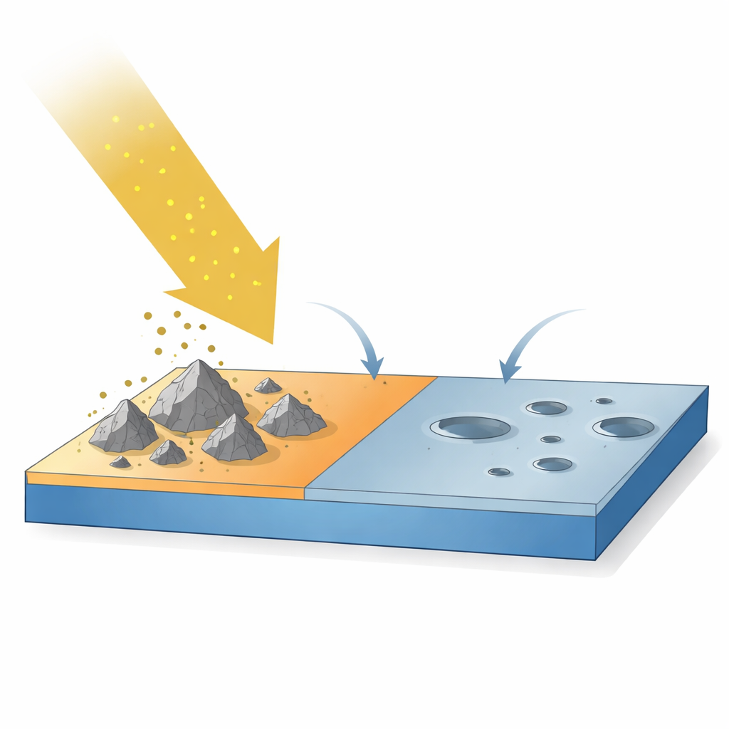
The researchers began by growing antimony films just 50 nanometers thick—about a thousand times thinner than a human hair—on single-crystal sapphire. They used a technique called molecular beam epitaxy, which lets atoms land gently and build up layer by layer. By simply changing the substrate temperature during growth, they created two very different starting landscapes. At higher temperature, the antimony did not form a flat sheet, but instead self-assembled into well-shaped nanocrystals that looked like tiny pyramids and triangles resting on the sapphire. At room temperature, by contrast, the film was continuous and grainy, with a worm-like texture. These two starting morphologies turned out to respond in strikingly different ways when exposed to ion beams.
Hitting the films with ion beams
To probe and tune the films, the team used a specialized setup that combines a scanning electron microscope with a particle accelerator. They blasted the samples with 2 MeV aluminum ions while watching the surface evolve in real time. At these high energies, ions mainly deposit energy into the electrons in the material, which very briefly heats up tiny cylindrical regions—so-called thermal spikes—along the ion path. For the high-temperature-grown film with isolated nanocrystals, the early stages of irradiation created disorder inside the crystals, effectively lowering antimony’s melting point. As the ion dose increased, parts of the pyramidal crystals locally melted and antimony atoms evaporated away, shrinking and blunting the square pyramids, while the triangular islands remained comparatively stable.
From rough film to ordered islands
The room-temperature-grown film behaved almost like the opposite case. Initially, it was a continuous but disordered layer with many small grains. As the ion dose rose, holes started to appear and grow in the film—evidence of dewetting, where a solid film retracts and breaks up into isolated patches, much like a liquid film beading up on a surface. At the same time, optical and electronic measurements showed that the film actually became more crystalline and more conductive after irradiation. Raman scattering revealed sharper vibrational peaks and less variation from place to place, while tunneling measurements showed that the electronic bandgap shrank and the electrical resistance dropped. Together, these signatures point to ion-induced crystallization triggered by the intense but fleeting heating during each thermal spike.

Invisible stress and hidden heat
To explain these transformations, the authors modeled how energy from each ion impact spreads and cools. Their calculations show that, in the region around the ion track, the lattice temperature in antimony can briefly exceed its melting point, while the sapphire remains solid. When this molten zone cools in a fraction of a trillionth of a second, it creates strong in-plane compressive stresses in the antimony layer—estimated around 0.34 gigapascals. In continuous, initially disordered films, this stress can help drive both crystallization and the nucleation of holes as the film pulls away from the substrate. In contrast, for isolated nanocrystals, repeated local overheating leads primarily to increased disorder and eventual evaporation from the crystal facets.
What this means for future devices
Taken together, the results show that ion beams are not just a tool for damaging materials—they can be used to selectively crystallize, disorder, reshape, or even partially remove nanoscale antimony structures, depending on how the film was prepared. This dual behavior—crystalline nanocrystals becoming disordered and eroded, while disordered continuous films become more crystalline and break up—highlights how sensitive ultrathin layers are to local heat and stress. Because antimony already shows promise as a fast-switching phase-change material for photonic and electronic applications, the ability to tune its state with ions opens another route to engineer memory elements and optical components. In principle, carefully designed ion treatments could precondition or pattern antimony films to optimize speed, power consumption, and reliability in next-generation information technologies.
Citation: Job, J., Jegadeesan, P., Gahlot, V.S. et al. In-situ ion irradiation investigations on MBE grown Sb thin films on sapphire. Sci Rep 16, 13475 (2026). https://doi.org/10.1038/s41598-026-39001-9
Keywords: antimonene, phase-change materials, ion irradiation, thin films, sapphire substrates