Clear Sky Science · en
Enhancing bonding strength of the electroplated Cu pillars for semiconductor package by controlling grain orientation
Why tiny metal towers matter for fast chips
Inside modern high‑performance computers and artificial‑intelligence hardware, memory chips must trade data at astonishing speeds. To do that, they rely on thousands of tiny metal towers, called copper pillars, that stand between a silicon chip and its package. These pillars carry electrical signals, conduct heat, and help hold the stack together. As engineers squeeze more connections into smaller spaces, each pillar becomes thinner and closer to its neighbors, making the strength of every single joint critically important. This study explores how a subtle change in the way these copper pillars are grown can make the difference between a robust, long‑lived package and one that may crack under stress. 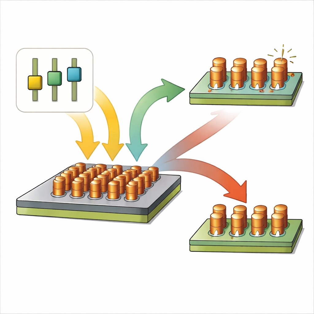
From solder bumps to copper towers
For years, flat blobs of solder were the standard way to connect a chip to its package. However, as the spacing between connections shrinks below about one‑tenth of a millimeter, these soft bumps lose height and crowd together, limiting performance and reliability. Copper pillars offer a more elegant solution: a rigid copper column topped with a thin solder cap. This rigid shape keeps a consistent stand‑off height, improves electrical and thermal behavior, and can be packed more densely. But the internal crystal pattern of the copper and the way its surface is shaped during manufacturing quietly govern how well each pillar stays attached when the device heats, cools, and flexes in use.
How making the metal changes its inner pattern
The researchers fabricated copper pillars just 25 micrometers wide—about a quarter of a human hair—with a fixed chemistry in the plating bath but three different electrical current settings during growth. Using electron microscopes and diffraction techniques, they mapped the tiny crystal grains inside each pillar. At the lowest current, the copper grew as relatively large, orderly columns dominated by one particularly stable orientation. As the current increased, the metal solidified more rapidly, producing much finer grains with a jumble of orientations. This refinement might sound beneficial, since small grains can strengthen metals, but it also produces many more internal boundaries where atoms are misaligned and more vulnerable to chemical attack.
Hidden notches that weaken the joint
After the pillars were grown, the team removed the temporary copper “seed” layer beneath them with an acid solution. Ideally, this step simply clears away unwanted metal, but in practice it can also gnaw sideways underneath the base of each pillar, carving a small recess known as an undercut. By examining cross‑sections, the scientists found that low‑current pillars developed only a shallow undercut, less than half a micrometer deep. High‑current pillars, with their finer grain network, showed much larger scooped‑out regions, up to nearly two micrometers. Because grain boundaries act as easy pathways for the etching liquid, having more of them made it easier for the solution to spread laterally and hollow out the base.
Measuring strength and mapping stress
To see how these shapes affect real‑world performance, the team pushed sideways on individual pillars until they failed, mimicking a harsh mechanical load. Pillars grown at low current with small undercuts held almost twice the force of those produced at the highest current. Microscopy of the broken joints revealed that strong pillars tended to tear within the copper itself, a ductile, energy‑absorbing failure. In contrast, pillars with large undercuts tended to separate right along the hollowed‑out edge, an adhesive failure that suggests a weak interface. Computer simulations of the three‑dimensional stress distribution confirmed that undercuts concentrate stress at the lower rim of the pillar, exactly where cracks were observed to start. 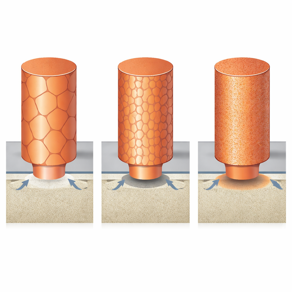
Designing sturdier connections for future chips
Overall, the study shows that, for these copper pillars, the biggest threat to reliability is not the basic strength of the metal but an irreversible geometric flaw carved in during etching. High‑current plating refines the grain structure yet encourages deep undercuts that sharply raise local stress and slash bonding strength. Low‑current plating fosters larger, more stable grains, resists undercut growth, and yields tougher joints. For chip makers, this means that carefully tuning the plating current—and future multi‑step current profiles—offers a practical path to pillars that keep next‑generation memory packages both fast and durable over years of operation.
Citation: Yoon, J., Shin, T., Kim, D. et al. Enhancing bonding strength of the electroplated Cu pillars for semiconductor package by controlling grain orientation. Sci Rep 16, 9814 (2026). https://doi.org/10.1038/s41598-026-38879-9
Keywords: copper pillar bumps, semiconductor packaging, electroplating, microstructure, mechanical reliability