Clear Sky Science · en
Localized carbon deposition enables trimming of photonic integrated circuits
Sharpening the paths of light on a chip
Light based chips promise faster data links and powerful optical computers, but they are hard to make perfectly. Tiny flaws that are invisible to the eye can nudge light off course and spoil performance. This study shows how placing minuscule patches of carbon on a chip with a focused ion beam can gently “retune” these light pathways after fabrication, helping future communication and computing hardware work closer to its design targets.
Why light circuits need careful touch ups
Photonic integrated circuits are chips that guide and process light instead of electric currents. They are central to fiber internet links, emerging quantum computers, and optical accelerators for artificial intelligence. Their function depends on carefully shaped waveguides that steer specific patterns of light. However, even slight variations in width or spacing introduced during mass production can shift how light travels, and these small errors add up as chips grow more complex. Engineers therefore rely on “trimming” methods, applied after fabrication, to bring devices back into tune without rebuilding the whole chip.
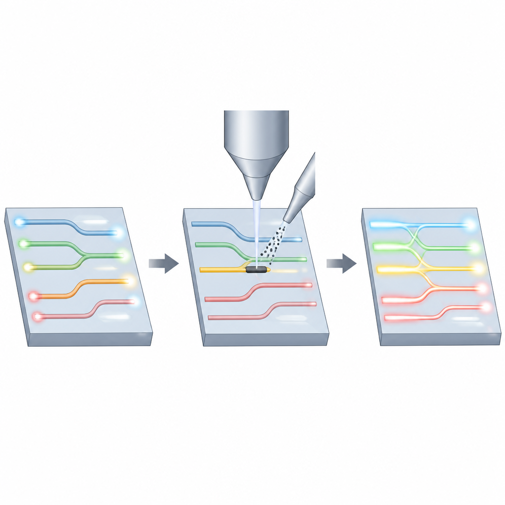
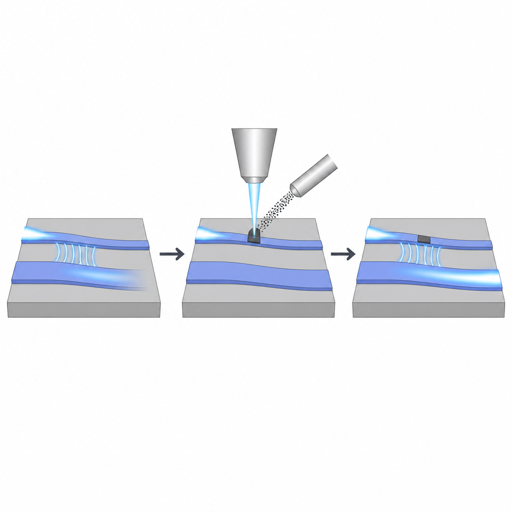
Adding carbon as a local tuning knob
The authors explore a trimming strategy that uses a focused ion beam to decompose a carbon containing gas right where it hits the chip surface. This deposits a narrow strip of diamond like amorphous carbon with nanometer scale precision, all at room temperature. The added layer slightly changes how light experiences the underlying waveguide: its effective refractive index increases, which in turn shifts how modes of light convert and interfere. Because the process only touches the surface and leaves the core of the light carrying material intact, it avoids the more drastic changes caused by methods that damage or melt the waveguide itself.
Testing the method on sensitive light splitters
To put this approach to the test, the team used asymmetric directional couplers, a type of on chip splitter that converts light from a simple pattern into a more complex one and back again. These devices are notoriously sensitive to fabrication errors, since they rely on precise matching between different light modes. By deliberately shifting one waveguide slightly out of its ideal shape, the researchers created couplers with extra loss. They then deposited carbon lines on the narrow waveguide and measured how the transmission changed. Both experiments and simulations showed that carefully chosen carbon geometry could restore the lost balance, cutting insertion loss from several decibels down to well under 1 decibel for some devices and offering tuning steps from about 1.5 to over 16 decibels across a set of samples.
Keeping losses low and performance stable
Any extra material added to a light path can introduce absorption, so the team quantified how much penalty the carbon brings. Simple test waveguides and interferometers revealed that the carbon layer adds about 76 decibels of loss per centimeter, but in the short trimmed regions used here this translates to only about 0.3 to 0.35 decibel for a standard phase shift, comparable to established non volatile trimming methods. Electron microscopy and spectroscopy confirmed that carbon and gallium from the ion beam stay confined to the thin deposited layer, with no detectable change in the underlying silicon nitride waveguide. Thermal tests showed that trimming performance remains essentially unchanged up to around 250 degrees Celsius, and long term measurements found the optical response settles after a short initial drift and then stays stable for weeks.
From single devices to complex optical processors
Because the focused ion beam can draw carbon patterns without any lithography masks, this method is flexible and well suited to research grade tuning. The authors demonstrate its usefulness by improving the behavior of more complex structures, including Mach Zehnder interferometers and photonic crossbar arrays used for matrix vector multiplication in optical AI accelerators. In these circuits, the trimmed couplers combine signals carried in different spatial modes with much lower loss, making better use of the available light.
What this means for future light based chips
In plain terms, this work introduces a precise, low power way to “touch up” light circuits after they are made by painting tiny carbon strokes where needed. It does not yet replace factory scale processes, but it shows that surface carbon patches can finely adjust critical components without harming the chip core and with modest added loss. As photonic chips grow larger and more intricate, such localized trimming tools could become important for turning nearly correct devices into fully functional ones, especially in experimental platforms pushing the limits of optical computing and communications.
Citation: Xu, R., Tang, Z., McRae, L. et al. Localized carbon deposition enables trimming of photonic integrated circuits. Nat Commun 17, 4562 (2026). https://doi.org/10.1038/s41467-026-73411-7
Keywords: photonic integrated circuits, focused ion beam, carbon deposition, optical trimming, asymmetric directional couplers