Clear Sky Science · en
Single-photon emission from two-dimensional perovskites channeled through low-energy edge states
Turning tiny crystals into single light sources
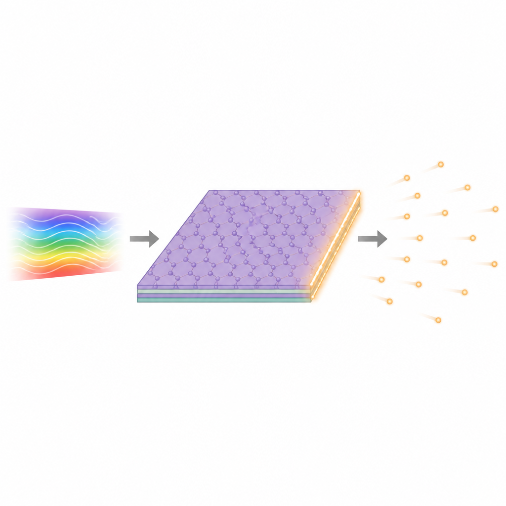
Sending information with single particles of light is one of the dreams of quantum technology, but building practical devices that spit out one photon at a time has been difficult. This study shows that a new class of thin, stackable crystals called two-dimensional perovskites can act as controllable single-photon sources when their outer edges are used in a clever way, pointing toward simpler components for future quantum communication circuits.
Why single photons matter for future tech
Secure quantum communication and some forms of quantum computing rely on streams of single photons that behave more like well-spaced marbles than like a continuous beam. Today, researchers get such light from defects in diamond, quantum dots, or special two-dimensional materials. Each platform has drawbacks, such as difficulty placing emitters exactly where they are needed or linking them efficiently to tiny optical circuits. The appeal of two-dimensional perovskites is that they are inexpensive, solution-processable, and easily integrated with other devices, yet their potential as quantum light sources had not been fully explored.
A special role for the crystal edges
The team focused on layered lead halide perovskites, which naturally form stacks of inorganic and organic sheets that act like built-in quantum wells. Earlier work had hinted that the edges of these sheets behave differently from their interiors, with distinct electrical and light-emitting properties. Using high-resolution electron microscopy, the authors confirmed that the interior has a regular lattice, while the edges are more disordered over a few nanometers. By carefully exfoliating bulk crystals into thin sheets with wide, terraced edges, they created samples where edge regions could be probed cleanly and compared directly to the flat interior.
Using gentle light to find hidden emitters
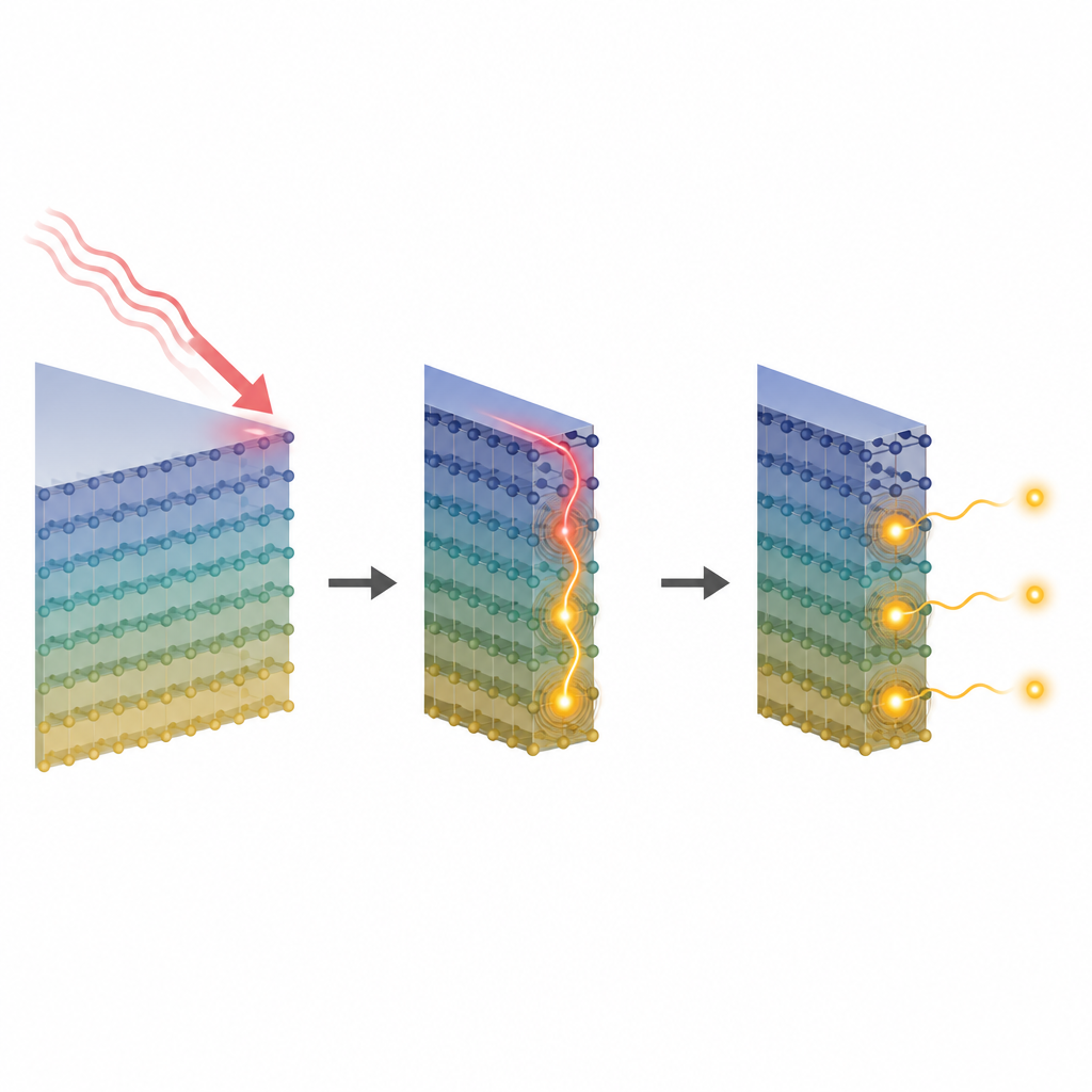
To test how these crystals respond to light, the researchers scanned them with tunable lasers at very low temperatures and at room temperature. When they used high-energy light, both the interior and edges mainly produced a broad glow typical of many overlapping processes, with no clearly isolated bright spots. As they dialed the light energy down toward and then below the crystal’s bandgap, a surprising pattern emerged: the interiors remained mostly uniform, but the edges lit up with a few sharply localized points. Detailed spectral measurements and photon-correlation tests showed that some of these tiny spots emitted light one photon at a time, a clear signature of single-photon sources.
Channels and deep traps inside the material
Follow-up measurements revealed how this works at the microscopic level. The edges host low-energy electronic states that sit below the main conduction band, acting as channels that guide excited charges toward even deeper defect sites in the bandgap. Under gentle, sub-bandgap illumination, charges are injected directly into these edge states and then funneled into rare deep traps that emit narrow, stable lines of light. Because other competing pathways are less active at these energies, the deep sites can release photons one by one at a high rate. Time-resolved experiments showed that these single-photon emitters are bright and fast, with lifetimes shorter than those in many other quantum-emitter materials.
Creating artificial edges with strain
The authors also explored how to position emitters where they are practically useful. They placed perovskite sheets on patterned polymer nanorods that stretch the crystal locally, creating edge-like distortions inside the flake. Under the same low-energy illumination, these strained regions produced localized emission spots with the same single-photon behavior seen at natural edges. By varying the thickness of the inorganic layers in the perovskite, they could shift the photon energy range, hinting that both composition and patterning can be used to fine-tune the emitters.
What this means for quantum devices
In simple terms, this work shows that two-dimensional perovskites can host tiny “light faucets” at their edges that drip out one photon at a time when tickled with just the right color of gentle light. Because these materials are easy to process from solution and can be patterned with strain or other techniques, they offer a flexible route to building arrays of quantum light sources on chips. The discovery that low-energy edge states can efficiently feed deep emitting sites provides a new design rule for engineering quantum emitters in layered materials and may help bridge the gap between laboratory demonstrations and practical quantum technologies.
Citation: Na, G., Park, J.Y., So, JP. et al. Single-photon emission from two-dimensional perovskites channeled through low-energy edge states. Nat Commun 17, 4317 (2026). https://doi.org/10.1038/s41467-026-71000-2
Keywords: single photon emission, 2D perovskites, edge states, quantum emitters, quantum optics