Clear Sky Science · en
Medium-scale integrated circuits based on p-type 2D semiconducting MoTe2
Smaller, Faster Electronics on the Horizon
As our gadgets shrink and grow more powerful, traditional silicon chips are starting to hit hard limits in size and energy use. This study explores a new ultra thin material that could help keep progress going: a sheet-like semiconductor only a few atoms thick that behaves as a key building block for future low power, high density electronics.
Why New Materials Are Needed
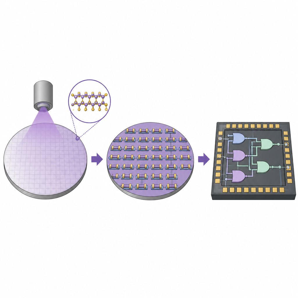
Modern electronics rely on silicon switches called transistors, packed by the billions on each chip. Pushing them to ever smaller sizes is becoming harder because of physical and manufacturing limits. Two dimensional materials, which are as thin as a single molecule yet sturdy and controllable, offer a fresh path. Many of these materials can already act as “n type” switches, which mainly move negative charges. To build full logic circuits, however, industry also needs equally good “p type” switches that handle positive charges. Until now, p type versions have worked only in tiny samples or as a few isolated devices, far from what a real chip factory needs.
Growing Atom Thin Films on Full Wafers
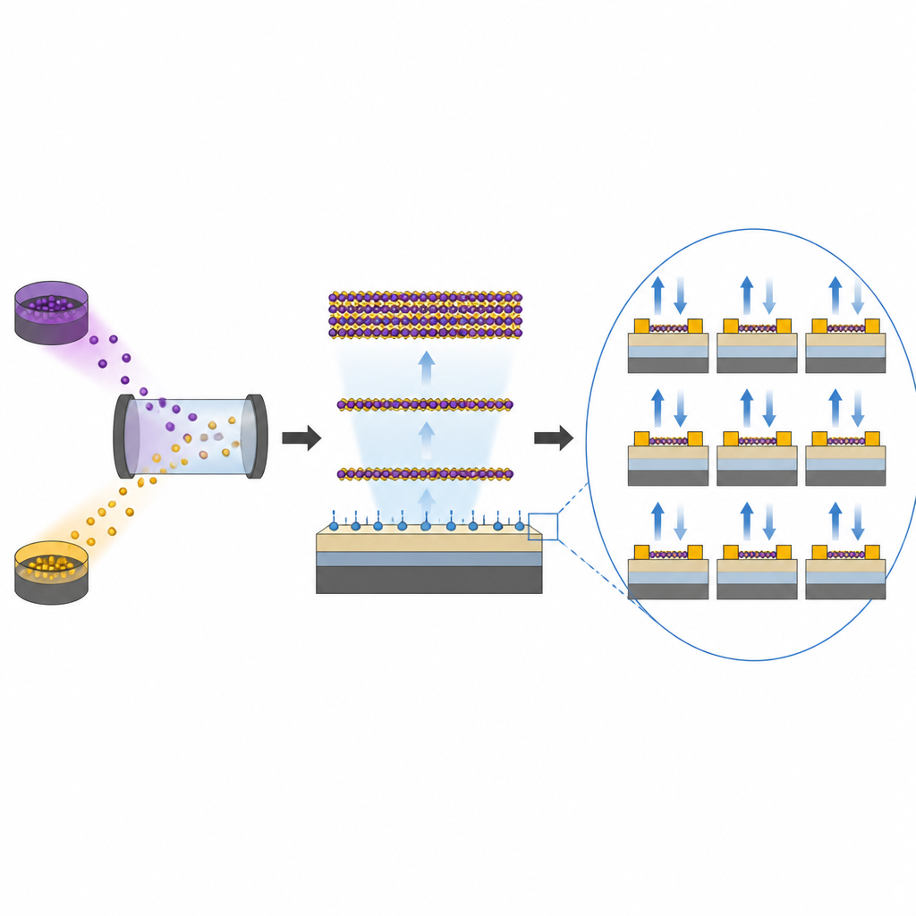
The researchers focused on a p type material called MoTe2, which can form extremely thin, smooth layers. Their challenge was to coat an entire 4 inch wafer with films only a few atomic layers thick, all with nearly identical thickness and quality from edge to edge. They redesigned the growth process in a gas filled furnace so that both ingredients, molybdenum and tellurium, reached the wafer in a steady, well balanced way. A key trick was turning the tellurium powder into a “slow release” source wrapped in porous beads, which keeps its vapor flow stable and prevents defects. At the same time, they treated the wafer surface with oxygen plasma so an ultrathin molybdenum layer wets it evenly instead of breaking into islands, allowing the final MoTe2 film to stay continuous even at just three layers thick.
Checking Uniformity from Atoms to Wafer
To confirm success, the team examined the films over many length scales. High resolution electron microscopes showed orderly atomic patterns and very few defects. Measurements of step height across the surface revealed that the layer count could be tuned from three to twenty simply by setting the starting metal thickness, and that the roughness stayed below the height of a single atom. They also probed 25 widely spaced spots on the wafer using light scattering methods and found that key signals hardly varied. Together, these tests indicate that the new growth recipe produces films that are not only wafer scale but also highly uniform, a crucial requirement for making thousands of nearly identical devices.
Turning Ultra Thin Films into Reliable Switches
Next, the group turned the films into practical transistors. They paired three layer MoTe2 channels with a thin layer of a so called high k insulating material, HfO2, which lets the gate electrode control the channel more strongly at low voltage. By carefully patterning the channels and metal contacts using standard chip making tools, they built dense arrays of p type transistors across the 4 inch wafer. These devices switch cleanly between on and off states, achieving on off current ratios around one hundred thousand while operating at only four volts. Statistical tests on one hundred devices showed that their switching points barely vary by more than a few hundredths of a volt, approaching the uniformity seen in advanced silicon technology.
From Simple Gates to Working Arithmetic
With a stable supply of matching transistors, the researchers assembled basic logic building blocks such as inverters, NAND, and NOR gates. These circuits produced clear digital highs and lows, could be chained together without signal loss, and ran ring oscillators whose steady pulse frequency revealed that the gates behave almost identically. Finally, they demonstrated a four bit full adder, a small arithmetic unit made of 140 p type MoTe2 transistors arranged in several layers of logic. This medium scale circuit correctly added pairs of four bit numbers in all tested cases, showing that the material and fabrication process can support deep, multi stage logic rather than just isolated tests.
What This Means for Future Chips
This work shows that atom thin p type MoTe2 can be grown over full industry style wafers and turned into many uniform, low voltage transistors and functional logic circuits. While the device sizes are still larger and slower than those in cutting edge silicon chips, the approach bridges a key gap between single experimental devices and truly integrated circuits. It suggests that two dimensional materials could one day join or complement silicon in building compact, energy efficient processors that keep the progress of electronics moving forward.
Citation: Wang, H., Luo, Z., Zheng, B. et al. Medium-scale integrated circuits based on p-type 2D semiconducting MoTe2. Nat Commun 17, 4320 (2026). https://doi.org/10.1038/s41467-026-70992-1
Keywords: 2D electronics, MoTe2, p type transistor, integrated circuits, wafer scale growth