Clear Sky Science · en
Cryogenic neuromorphic circuits using gate-controlled negative differential resistance in silicon carbide
Why freezing cold computers matter
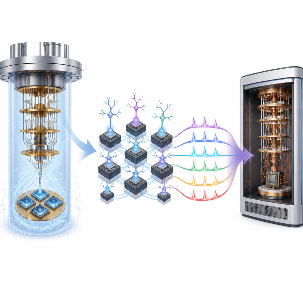
Quantum computers and ultra-sensitive space instruments must run close to absolute zero, where even a tiny bit of waste heat can cause trouble. Engineers therefore need electronic circuits that can think and react while using almost no power at all. This study shows how a familiar semiconductor material, silicon carbide, can be turned into tiny neuron-like building blocks that work reliably in this deep-freeze environment and may help control future quantum machines.
A new twist on a familiar transistor
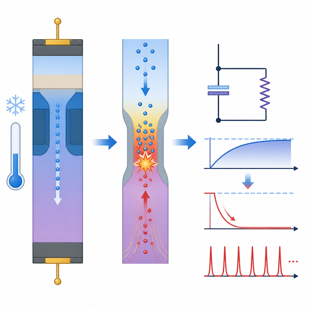
The researchers start with a vertical silicon carbide transistor, a workhorse device already manufactured on large industrial wafers. When they cool this transistor to temperatures below about 2 kelvin, its current–voltage behavior changes in a striking way. Instead of current simply rising with voltage, there is a region where increasing voltage actually makes the current drop. This counterintuitive effect, called negative differential resistance, creates a natural switching behavior: the device can jump between a very low-current state and a very high-current state with an on/off ratio of more than ten million, while still leaking almost no current when it is off.
How cold electrons create sharp switching
At such low temperatures, most electrons in the interior of the transistor are trapped on impurity atoms and do not move, so the device barely conducts. When a gate voltage is applied, it opens a path for electrons to flow from a heavily doped source region into a lightly doped region. There, strong electric fields cause some electrons to knock others free from their impurity sites, a process known as impact ionization. Because silicon carbide contains two closely spaced donor energy levels from nitrogen atoms, this chain reaction switches on very abruptly and then saturates, giving the characteristic S-shaped curve of negative differential resistance. Crucially, the position and width of this switching region can be tuned simply by adjusting the gate voltage, turning the device into a highly programmable element.
Turning devices into artificial cold neurons
Using this controllable switching, the team builds several types of neuromorphic circuits that mimic different behaviors of biological neurons. In a sensory neuron circuit, a resistor and capacitor slowly charge the transistor until it reaches the switching threshold, then the negative differential resistance causes a rapid discharge, creating a sharp voltage spike. Repeating this cycle generates a train of spikes whose rate depends on the input signal and circuit values, much like real sensory nerves that fire faster in response to stronger stimuli. Because the switching is governed by stable material properties rather than heat, the spiking remains robust over many cycles and across different devices and wafer batches.
Logic and memory at a fraction of the power
The same building block can perform logic and memory-like functions. By feeding pulses into a small capacitor and then briefly enabling the transistor, the circuit can act as a spiking version of OR or AND gates, depending on the chosen control voltage. In another configuration, the device serves as an integrate-and-fire neuron, adding up incoming spikes until a threshold is reached and then emitting a strong output spike. The researchers demonstrate both positive and negative variants so that the output of one stage can directly drive the next, and they show cascaded chains of these neurons operating stably at temperatures around one tenth of a kelvin.
From laboratory demo to cryogenic brains
Although the experiments use relatively large, discrete components, the authors estimate that a fully integrated version on a silicon carbide chip could shrink each neuron to a few hundred square micrometers and reduce energy use per spike to just tens of femtojoules. Because silicon carbide processing is already mature in industry, this approach could scale to many devices on a wafer and coexist with other cryogenic components. In simple terms, the work points to a way of building tiny, brain-inspired control circuits that scarcely warm their surroundings, making them well suited to manage delicate quantum bits, cold sensors, and space instruments operating at the edge of absolute zero.
Citation: Yang, X., Porter, M., Qin, Y. et al. Cryogenic neuromorphic circuits using gate-controlled negative differential resistance in silicon carbide. Nat Commun 17, 4351 (2026). https://doi.org/10.1038/s41467-026-70963-6
Keywords: cryogenic electronics, silicon carbide, neuromorphic circuits, negative differential resistance, quantum computing control