Clear Sky Science · en
Point defects in monolayer WSi2N4 and MoSi2N4
Tiny flaws with big effects
Electronics are built from crystals so thin that they can be just one atom thick. In such delicate sheets, even a single misplaced or missing atom can change how electricity and heat flow. This study looks closely at those tiny flaws in two new ultra-thin semiconductors and shows how they can be turned from an unwanted nuisance into a powerful design tool for future devices.
A new family of ultra thin crystals
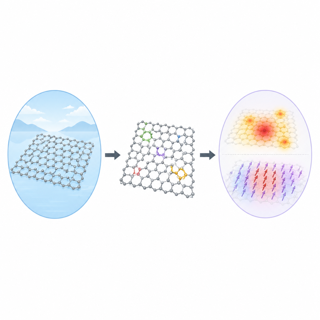
The work focuses on a recently discovered family of materials called MoSi2N4 and WSi2N4. Each one is a single, sandwich like stack of seven atomic layers made of metal, silicon, and nitrogen. These sheets are strong, conduct heat well, and already have better electrical performance than many well known two dimensional materials. Because of their complex structure, they can host many different kinds of atomic flaws, which offers more ways to tune their behavior than in simpler sheets like graphene.
Seeing single atoms go missing
To find out exactly what kinds of defects appear, the researchers used advanced electron microscopes that can see individual atoms. By combining two imaging modes that are sensitive to light and heavy elements, plus computer simulations and quantum calculations, they mapped out ten distinct types of point defects in monolayer WSi2N4 and confirmed that similar ones appear in MoSi2N4. Some defects are vacancies, where one or more nitrogen, silicon, or tungsten atoms are missing. Others are antisites, where an atom sits in the wrong kind of site, such as a silicon atom taking the place of a nitrogen atom. They also counted how often each defect appears and linked these counts to how easily each defect forms during crystal growth.
How defects reshape electrical and magnetic behavior
Next, the team asked how these tiny flaws change the way electrons move. Using first principles quantum calculations, they showed that many of the common defects shrink the energy gap that makes these materials semiconducting, and several close it completely so the sheet behaves like a metal. Some defects introduce localized electronic states that act like traps, slowing down charge motion and lowering mobility. Others, such as certain silicon on nitrogen sites, can actually raise hole mobility compared with the perfect crystal. A subset of defects creates spin polarized electronic bands, giving rise to small magnetic moments around the defect sites. Scanning tunneling measurements on real samples confirmed that specific defects reduce the local bandgap or even produce metallic regions, matching the theoretical predictions.
When flaws link up into lines and networks
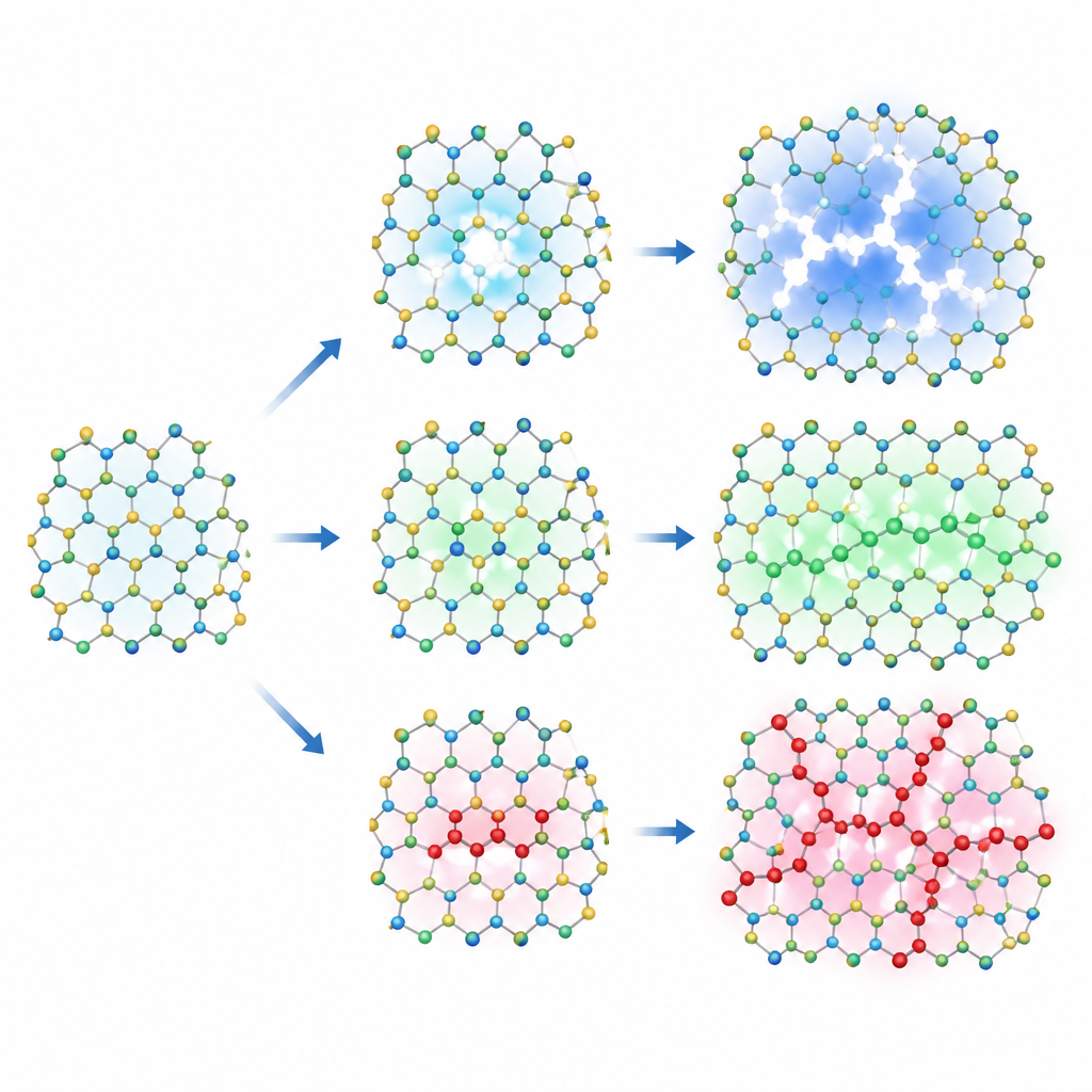
Beyond isolated imperfections, the researchers found that some defects tend to gather into ordered patterns. In MoSi2N4, repeated silicon on nitrogen substitutions can form two dimensional networks that sit like a flat fault plane within the sheet, while pairs of silicon atoms replacing a metal atom assemble into one dimensional chains. Calculations show that these extended structures are energetically favored and form during high temperature growth. They strongly reshape the electronic band structure, again narrowing or closing the gap and adding new electronic states that are mainly tied to the substituted atoms along the network or chain.
Designing devices by tuning imperfections
Together, these results turn defects from a vague problem into a detailed design toolkit. By choosing growth conditions that favor certain vacancies or substitutions, engineers could locally turn parts of a WSi2N4 or MoSi2N4 sheet more metallic to improve electrical contacts, introduce magnetic regions for spin based devices, or adjust heat flow and light absorption. In plain terms, the study shows that carefully placed atomic flaws in these ultrathin crystals can be used to draw custom electronic pathways and magnetic patches at the scale of single atoms.
Citation: Tong, J., Cao, Y., Wang, YK. et al. Point defects in monolayer WSi2N4 and MoSi2N4. Nat Commun 17, 4319 (2026). https://doi.org/10.1038/s41467-026-70946-7
Keywords: two dimensional semiconductors, atomic defects, MoSi2N4, WSi2N4, defect engineering