Clear Sky Science · en
Photoresist-guided indirect photopatterning of quantum dots via carbene-mediated ligand thermocrosslinking
Sharper Screens for Future Headsets
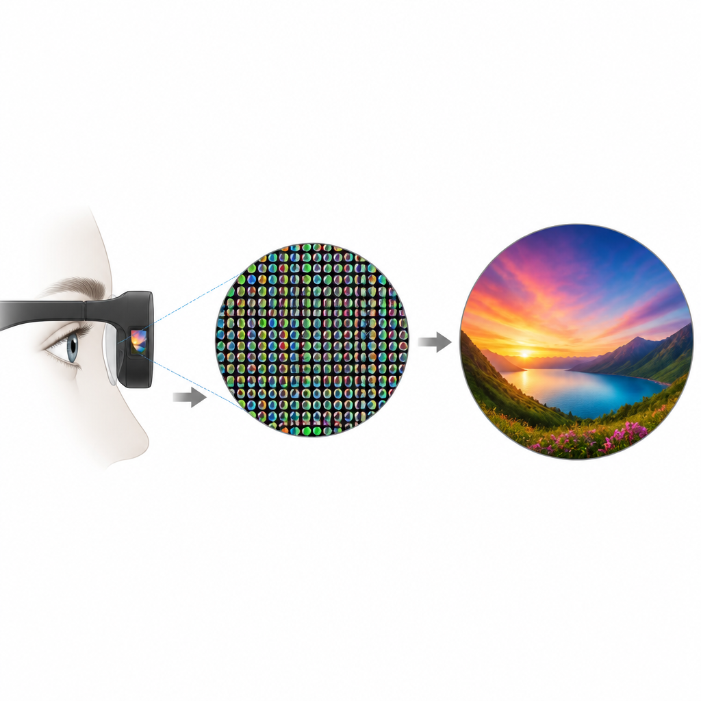
When you strap on a virtual or augmented reality headset, any tiny flaw in the screen is magnified right in front of your eyes. One of the most distracting flaws is the “screen door” effect, where the gaps between pixels become visible as a faint grid. This study shows a way to build ultra‑dense, highly colorful pixels using quantum dots so that these gaps nearly disappear, paving the way for smoother, more comfortable immersive displays.
Why Tiny Light Pixels Matter
Head‑mounted displays sit just a few centimeters from the eye, so their screens must pack in far more pixels per inch than a television or phone. To avoid visible pixel boundaries and reduce motion sickness, engineers aim for more than 3000 pixels per inch, meaning each red, green, and blue subpixel is only a few micrometers across. Quantum dots, nanometer‑scale crystals that emit pure and tunable colors, are ideal for these tiny light sources, but making sharp, reliable patterns of them at this scale without harming their brightness is a major challenge.
Limits of Existing Patterning Methods
Conventional chip‑style patterning methods carve shapes out of a material using harsh etching or intense light. Quantum dots, with their large exposed surfaces, can lose brightness or change color under these conditions. Some newer approaches try to pattern them directly with light, skipping the etching step, but the needed high‑energy exposure can still damage the dots and tends to produce edges that are rough at the nanoscale. Rough edges may sound minor, but at micrometer sizes they blur pixel boundaries, limiting how sharp and dense the display can be.
A Gentle Three Step Patterning Trick
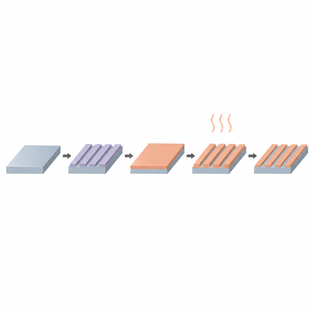
The researchers introduce a “photoresist guided indirect” patterning method that rearranges the usual steps to protect the quantum dots. First, they make sacrificial patterns from a standard photoresist, the same kind of light sensitive material used in the chip industry. Next, they coat these patterns with a thin film of quantum dots mixed with a specially designed helper molecule called Diazo‑4‑LiXer. When the film is gently heated to around 110 degrees Celsius, this helper generates short lived reactive species that stitch the organic shells of neighboring dots together, forming a solid, solvent resistant network. Finally, the sacrificial photoresist is washed away, taking the unwanted parts of the film with it and leaving behind sharply defined quantum dot lines or dots.
Keeping the Dots Bright and the Edges Clean
A key achievement is that this stitching reaction works at relatively low temperatures and does not require intense ultraviolet light. That means the supporting photoresist keeps its normal behavior and can be fully removed, while the quantum dots retain their original color and brightness. Measurements of surface profiles show that the resulting quantum dot features have extremely smooth edges compared with direct light based methods, with record low roughness at micrometer scales. The team patterned red, green, and blue quantum dots separately, repeating the process multiple times on the same chip without noticeably degrading earlier layers, and achieved pixel densities above 4000 pixels per inch in full color arrays.
From Lab Steps to Working Displays
To prove that the method is more than a patterning trick, the authors built complete quantum dot light emitting devices. They integrated the patterned red, green, and blue regions into a 10 by 10 pixel passive matrix display and showed that the electrical performance and brightness match those of devices made without the extra patterning steps. The crosslinked quantum dot layers remained stable through the repeated coating, heating, and washing cycles needed for full color fabrication, and the test displays produced bright, uniform images under different driving conditions.
What This Means for Everyday Devices
In simple terms, the work demonstrates a way to “lock” quantum dots into precise, damage resistant patterns using a gentle chemical stitch, while keeping them as bright and efficient as before. Because the process is compatible with existing photolithography tools already used in display factories, it offers a practical path toward ultra‑high‑resolution, quantum dot based screens for virtual and augmented reality headsets and other compact devices where every micron of screen area counts.
Citation: Kim, H., Ham, H., Lim, C.H. et al. Photoresist-guided indirect photopatterning of quantum dots via carbene-mediated ligand thermocrosslinking. Nat Commun 17, 4162 (2026). https://doi.org/10.1038/s41467-026-70770-z
Keywords: quantum dot displays, microdisplay patterning, virtual reality screens, photolithography, high resolution pixels