Clear Sky Science · en
Generic logic block based on bias-gated 2D MoS2 transistors
Smaller, Smarter Computer Brains
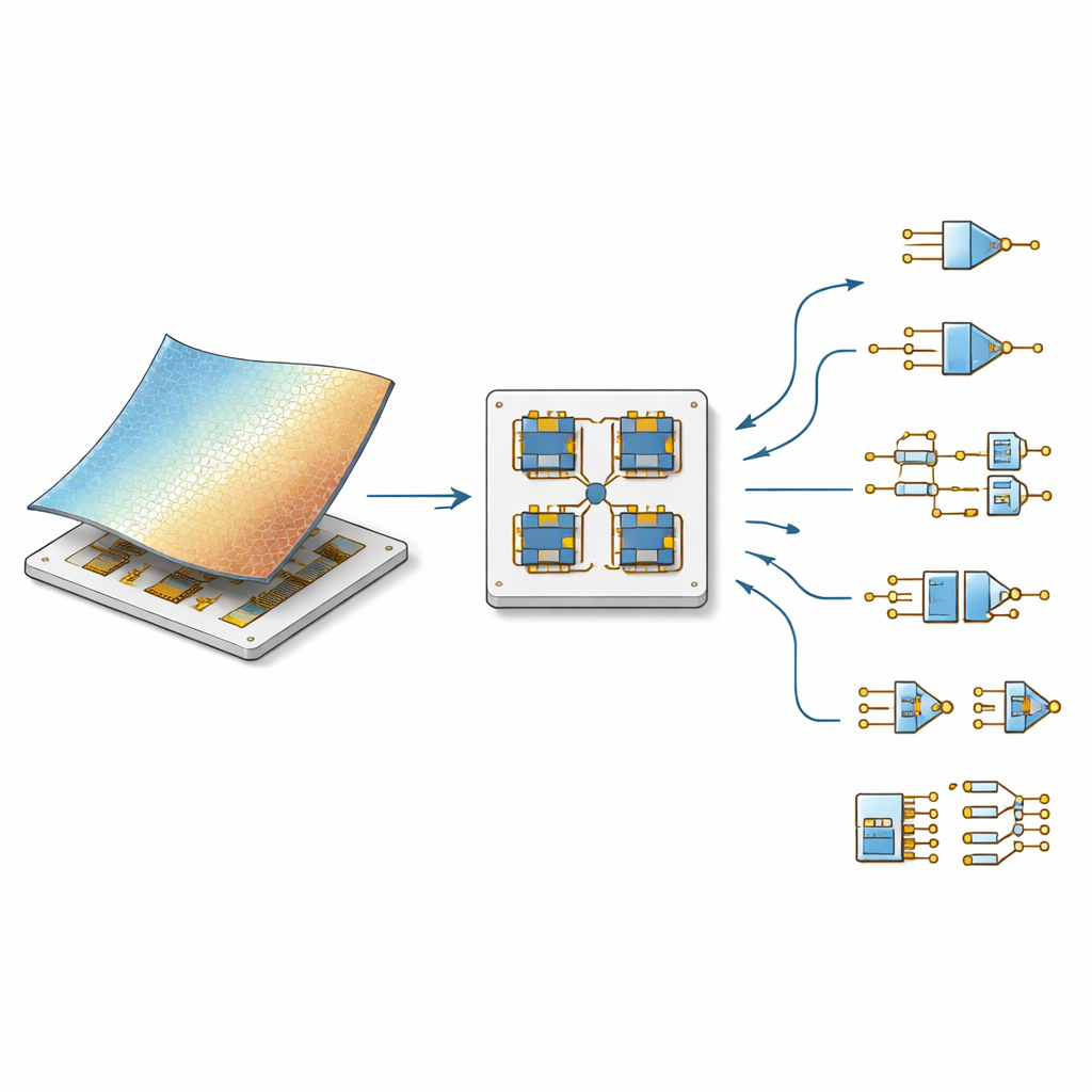
Modern chips pack billions of tiny switches called transistors, but shrinking them further is getting harder and more expensive. This study shows a new way to build logic circuits using an ultra-thin material only a single molecule thick. With a clever transistor design, the researchers compress many different digital operations—like adding numbers and storing bits—into a single, reusable building block. That could help future electronics become more powerful, more compact, and more energy‑efficient.
A New Kind of Switch
The work centers on a material called molybdenum disulfide, or MoS2, which forms stable sheets only one atom thick. Such two‑dimensional layers can keep excellent electronic performance even when devices are shrunk to extreme scales, making them attractive candidates for future chips. The challenge is that standard silicon technology relies on heavy chemical doping to create complementary “on” and “off” behaviors, but there is almost no room to insert dopant atoms into an atom‑thin crystal. As a result, most circuits built from 2D materials so far have been simpler, less efficient designs that consume more power and use many transistors to achieve basic logic functions.
Controlling Behavior with a Gentle Nudge
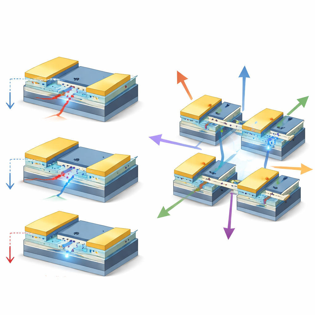
Instead of changing the material’s chemistry, the team reshapes how electric fields act inside each transistor. Their device, called a bias‑gated field‑effect transistor (BG‑FET), sandwiches a monolayer of MoS2 between carefully chosen insulating layers and adds an extra metal electrode that extends asymmetrically over one side of the channel. By choosing whether this special electrode sits at the source or the drain contact and by adjusting its voltage, the researchers can shift how easily electrons enter or leave the channel. This effectively changes the transistor’s switching threshold on demand, without altering the material itself. Measurements on large arrays of these devices show that this behavior is uniform, stable over weeks, and robust even at elevated temperatures.
From Single Switches to Working Circuits
To demonstrate usefulness in real logic, the researchers first built an inverter—the most basic digital element that flips a “0” to a “1” and vice versa—using two BG‑FETs with identical geometry. Simply operating one device in one bias mode and the other in the opposite mode produced a clean, full‑range output suitable for connecting many stages together. The inverter showed strong gain, low static power, and reliable switching over thousands of cycles, comparable to the best 2D‑material inverters made with more complicated, specially tuned devices. This showed that the adjustable threshold of BG‑FETs could be harnessed to simplify circuit design.
One Block, Many Digital Tricks
The core achievement is a “generic logic block” or GLB built from just four identical BG‑FETs. In this compact circuit, each transistor can be reprogrammed electronically, with interchangeable input and output terminals. By feeding in different combinations of control voltages, the same physical block can act as many different logic functions: basic gates such as AND, OR, and XOR; arithmetic units like a half‑adder and a multiplexer; and even a tiny memory cell similar to static RAM. Conventional complementary silicon technology would typically require more than a hundred separate transistors to realize the same collection of functions, whereas the GLB accomplishes it all within a single, reusable unit.
Building Larger Digital Machines
Because the GLB is a flexible building block, several of them can be chained together to create more complex digital hardware. The team combined four GLBs and a few inverters to build a two‑bit multiplier that computes the product of two small binary numbers, a common operation in processors and signal‑processing chips. They also assembled sequential elements that handle time‑dependent data, including latches and flip‑flops that respond to clock signals and can divide frequency. Across these examples, the number of BG‑FET devices needed was reduced by more than 60 percent compared with standard designs, hinting at major savings in chip area and wiring complexity.
What This Could Mean for Future Chips
In plain terms, this research shows that a single, cleverly designed switch made from an atom‑thin material can be turned into a “multi‑tool” for digital logic. Rather than hard‑wiring each operation with its own dedicated transistor cluster, the same tiny block can be reconfigured on demand to add, route, or store data. If integrated at large scale, such bias‑gated MoS2 logic blocks could enable smaller, more adaptable chips that continue the progress of miniaturization even as traditional silicon approaches its limits.
Citation: Wei, X., Chen, Z., Chen, K. et al. Generic logic block based on bias-gated 2D MoS2 transistors. Nat Commun 17, 3998 (2026). https://doi.org/10.1038/s41467-026-70712-9
Keywords: two-dimensional semiconductors, MoS2 transistors, reconfigurable logic, integrated circuits, post-CMOS technology