Clear Sky Science · en
High-κ KBe2BO3F2 dielectric material with wide bandgap for two-dimensional electronics
Why smaller, cooler chips matter
From smartphones to data centers, our gadgets rely on tiny electronic switches called transistors. As engineers keep shrinking these switches to fit more onto a chip, they fight a growing problem: wasted energy leaking through the insulating layers that control the current. This study introduces a new insulating material that could help future ultra-thin electronics run with less power and less heat, keeping our devices faster and more efficient.
A new kind of insulating layer
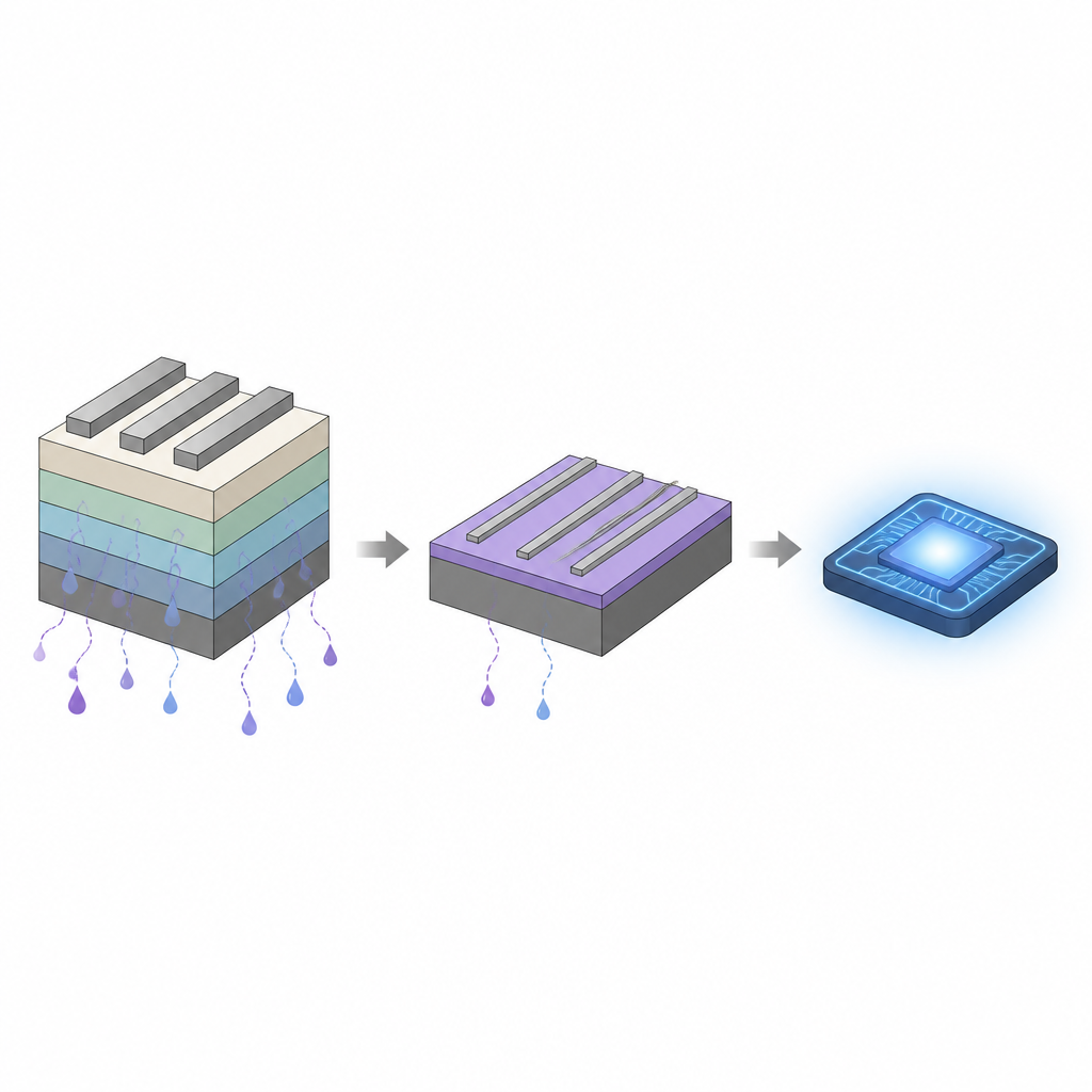
Modern transistors need an insulating layer that does two jobs at once: it must store electric charge well so the gate can easily turn the current on and off, and it must block electrons from sneaking through when they are supposed to stay put. These two traits usually work against each other. Materials that store charge well often let more current leak, while very good blockers store less. The researchers focused on a crystal called KBe2BO3F2, or KBBF, whose atoms are arranged in tightly bound layers containing very short chemical bonds and strongly charged elements. This special bonding gives KBBF both strong charge response and a very wide energy barrier against leaking electrons.
Peeling crystals into ultra-thin sheets
To use KBBF in cutting edge devices, the team needed it in ultra-thin form, only a few atoms thick. They used a mechanical method that gently slides and peels layers from a bulk crystal, a bit like separating pages in a stuck-together book. Microscopy images show that the peeled KBBF sheets are flat, uniform, and largely free of defects. When these sheets are stacked together with a common 2D semiconductor called MoS2, the boundary between them remains clean and smooth. There is even a tiny natural gap at the interface that further helps block unwanted tunneling of charges from the transistor gate into the channel below.
Measuring how well it stores and blocks
The team sandwiched KBBF sheets between metal layers to build simple test capacitors and directly measured how much charge they could hold and how stable that charge remained. Even when thinned down to just a few nanometers, KBBF kept a high ability to store charge, corresponding to a dielectric constant much larger than that of the common insulator used in today’s chips. At the same time, computer calculations and optical tests showed that KBBF has a very wide “bandgap,” an energy barrier above 8 electron volts that keeps electrons confined. This combination leads to extremely low leakage currents well below industry targets and a breakdown strength several times better than standard silicon dioxide, meaning KBBF can withstand high voltages for long periods. Lifetime tests suggest that devices using it could operate for about a decade at realistic voltages without the insulating layer failing.
Building and testing 2D transistors and circuits
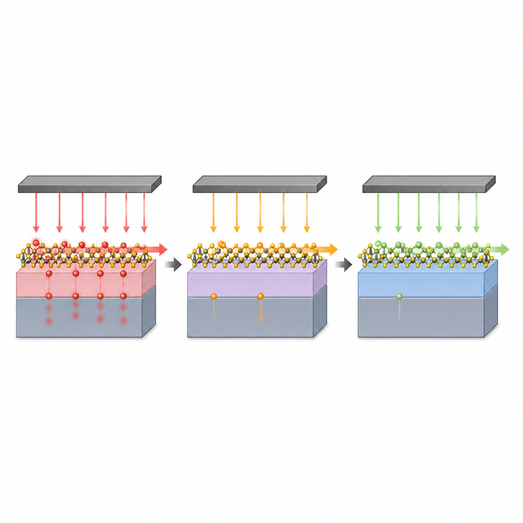
Armed with this new insulator, the researchers built transistors with MoS2 channels controlled from above by a thin KBBF sheet. These devices switched current on and off with remarkable sharpness, reaching the theoretical limit for how quickly a transistor can turn on at room temperature. They also maintained a huge ratio between on and off current while keeping unwanted gate leakage extremely low. Careful analysis indicates that the KBBF–MoS2 interface introduces very few electronic traps, and its ions stay fixed rather than drifting under stress, which keeps the switching behavior stable over time. The team further pushed the design to very short channels and even built a simple logic inverter circuit, which showed large signal gain and continued to work even at very low supply voltages.
What this means for future electronics
In everyday terms, the study shows that KBBF acts as a very thin but very strong electrical fence: it lets the transistor’s gate control the channel firmly while stopping almost all stray current from slipping through. This dual strength could help future two-dimensional electronic chips pack more transistors into a small area without paying a heavy price in wasted energy and heat. While KBBF itself contains beryllium and may not be the final commercial choice, it demonstrates a design path for new insulators that could keep the progress of smaller, cooler, and more efficient electronics on track.
Citation: Xu, Y., Liu, K., Peng, G. et al. High-κ KBe2BO3F2 dielectric material with wide bandgap for two-dimensional electronics. Nat Commun 17, 4301 (2026). https://doi.org/10.1038/s41467-026-70711-w
Keywords: two dimensional electronics, high k dielectric, wide bandgap insulator, MoS2 transistor, low power chip