Clear Sky Science · en
3D electron diffraction—the missing slice completing nanoscale analysis of organic solar cells in TEM
Why peeking inside solar cells matters
Solar panels based on carbon-based (organic) materials promise lightweight, flexible, and printable devices, but their performance depends sensitively on how molecules arrange themselves on the nanometer scale. Until now, scientists have had to choose between techniques that see average structure over large areas and methods that zoom in on tiny regions, making it hard to get a complete picture. This paper introduces a way to fill that gap: a three-dimensional form of electron diffraction that can be run inside a transmission electron microscope (TEM), tying together detailed images of the solar cell’s internal landscape with precise structural measurements.
Seeing more than blurry averages
Most currently used tools to study organic solar cells, such as grazing-incidence wide-angle X‑ray scattering (GIWAXS), work by shining X‑rays at a shallow angle onto thin films and reading the resulting diffraction pattern. GIWAXS is powerful: it tells researchers how closely molecules pack, how large their ordered regions are, and how well they line up, all while averaging over areas similar to the size of a pinhead. But it cannot directly show the real-space shapes of domains, local differences in orientation, or chemical variations within the film. It also inherently misses some information about purely in‑plane molecular arrangements because the probing geometry cannot look exactly along the film surface.
Adding the missing slice with electrons
The authors demonstrate that a complementary method—three-dimensional electron diffraction (3D ED)—can recover essentially the same structural parameters as GIWAXS while also supplying the missing pieces. In a TEM, a thin, free-standing solar-cell film is placed in the electron beam and tilted through many angles, with a diffraction pattern recorded at each step. These patterns are then reconstructed into a three-dimensional map of how the film scatters electrons. Using a well-studied model blend of a small-molecule donor and a fullerene acceptor (DRCN5T:PC71BM), the team shows that 3D ED reproduces key quantities such as lattice spacings, the effective size of ordered regions, and the spread of molecular orientations with remarkable agreement to both lab-based and synchrotron GIWAXS. 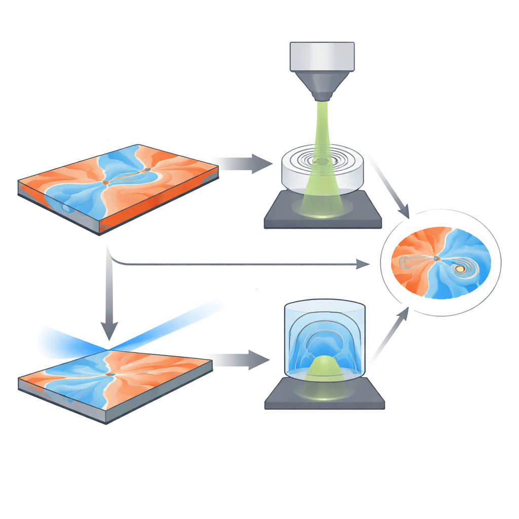
Linking structure to function, nanometer by nanometer
Because 3D ED lives inside the TEM, it can be combined seamlessly with imaging and spectroscopy. The authors exploit this to build a correlative picture of organic solar cells that connects molecular packing to visible domain shapes and composition. In the DRCN5T:PC71BM blend, elemental maps reveal “leaf-shaped” donor-rich regions embedded in the acceptor matrix. Diffraction imaging shows that within these leaves, many smaller crystallites are slightly misaligned with each other, forming a mosaic. The orientation of the tightly stacked molecular planes changes from region to region: some domains are “edge-on,” favoring charge transport along the plane of the film, while others are “face-on,” favoring vertical transport. By reconstructing the 3D diffraction volume, the team quantifies this mixture of orientations (texture) and the amount of spread around the preferred direction (mosaicity), then relates these metrics directly to the nanoscale morphology. 
Watching structure evolve with processing
To test how broadly the method applies, the researchers turn to a classic polymer-based blend, P3HT:PC71BM, and compare films before and after a short thermal annealing step. 3D ED reveals that heating sharpens particular diffraction rings linked to lamellar stacking of the polymer, indicating larger and more ordered crystallites, especially along certain directions. Additional diffraction imaging confirms that domains become more elongated and phase separation coarsens, trends that are known to improve device performance in this system. Even for this more beam-sensitive material, careful control of electron dose and energy filtering allows 3D ED to track structural evolution without destroying the underlying order, highlighting its practicality for a wide range of organic and hybrid thin films.
What this means for future solar cells
Taken together, the work shows that 3D electron diffraction can act as the “missing slice” in the structural analysis of organic solar cells. It delivers quantitative information comparable to GIWAXS while adding true three-dimensional orientation data and direct registration with real-space images and chemical maps in a single instrument. Rather than replacing X‑ray methods, 3D ED complements them, offering high sensitivity to in‑plane order and the ability to probe micrometer-sized regions in detail. As detector technology and automated workflows improve, this approach should help researchers systematically link processing conditions, nanoscale structure, and device performance—accelerating the design of more efficient and stable next-generation solar cells.
Citation: Kraus, I., Wu, M., Rechberger, S. et al. 3D electron diffraction—the missing slice completing nanoscale analysis of organic solar cells in TEM. Nat Commun 17, 3159 (2026). https://doi.org/10.1038/s41467-026-70690-y
Keywords: organic solar cells, 3D electron diffraction, transmission electron microscopy, GIWAXS, nanostructured thin films