Clear Sky Science · en
Probing boron vacancy defects in hBN via single spin relaxometry
Listening to Tiny Magnetic Whispers
As electronic devices and quantum technologies shrink toward the atomic scale, imperfections in materials stop being minor flaws and start acting like powerful tools. This study shows how a single atomic-scale sensor in diamond can “listen” to the magnetic whispers of hidden defects in an ultrathin material, revealing where they are and how they behave—without ever needing to see them glow with light. The work opens a path to characterizing quantum-ready defects that are too dim or too small for conventional microscopes.
A New Kind of Atomic-Scale Stethoscope
Many promising quantum technologies rely on tiny spins—minute magnets associated with individual electrons or nuclei—that can sense magnetic fields, temperature, strain, or electric fields at the nanoscale. One of the best-studied of these is the nitrogen-vacancy (NV) center in diamond, a point defect whose quantum state can be controlled and read out with lasers and microwaves at room temperature. But NV centers buried tens of nanometers below a diamond surface sit relatively far from the objects we want to probe, and diamond’s optical properties make it hard to collect all the light they emit. Researchers are therefore looking to atomically thin materials, where spin defects live right at the surface and can talk directly to their surroundings.
Why Boron Vacancies in an Ultrathin Crystal Matter
Hexagonal boron nitride (hBN) is a two-dimensional material—essentially a stack of atomically thin sheets—that uniquely hosts optically active spin defects. One important defect is the boron vacancy: a missing boron atom that turns a spot in the lattice into a controllable quantum magnet. These vacancies could act as quantum sensors on chip surfaces or inside future devices. However, existing tools struggle to show where these spin-active vacancies are, which charge state they are in, and how densely they are packed. Optical methods cannot easily distinguish the useful negatively charged vacancies from neutral ones, and they blur over a half-micrometer or more, washing out nanoscale details that matter for quantum performance.
Reading Spins Indirectly Through Relaxation
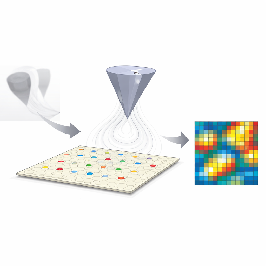
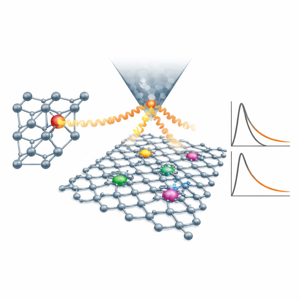
The authors solve this problem by using one quantum defect to probe another. They mount a diamond tip containing a single NV center on a scanning probe, positioning it about ten nanometers above hBN samples filled with boron vacancies. Instead of shining light on the hBN defects themselves, they monitor how the NV’s own spin relaxes—how quickly it forgets the state it was prepared in. By adjusting an external magnetic field, they tune the NV’s resonance frequency so that it matches that of the boron vacancies. At these “cross-relaxation” conditions, magnetic interactions cause the NV to exchange energy with nearby vacancies, shortening its relaxation time in a way that depends on how many active defects sit underneath.
Zooming In on Structure and Charge at the Nanoscale
Using this approach, the team performs several key measurements. In isotopically engineered hBN—where the nuclear makeup is carefully controlled—they resolve fine splittings in the vacancy’s resonance, fingerprints of nearby nuclear spins that affect magnetic behavior and sensing capability. By scanning the NV tip over hexagonal boron nitride grown with varying thickness, they turn changes in the NV’s relaxation into a quantitative map of defect density with roughly 100-nanometer pixels and potential for ten-nanometer resolution. Comparison with simulations shows that only a small fraction, about a few percent, of the total boron vacancies are in the negatively charged, spin-active state that can serve as quantum sensors. This charge selectivity is something standard optical or structural probes cannot easily provide.
Advantages Over Conventional Optical Readout
The relaxometry method offers both practical and conceptual advantages. It does not rely on collecting faint light from the boron vacancies themselves, which typically emit at wavelengths where standard detectors are inefficient and often show weak, low-contrast signals. Instead, the bright, well-understood fluorescence of the NV center acts as a universal readout channel. The same NV sensor can, in principle, probe a wide variety of spin defects—even optically dark ones or those emitting in telecom bands—simply by tuning the magnetic field until cross-relaxation occurs. Although building up full relaxation curves takes longer than simple continuous-wave optical measurements, the much higher contrast and the possibility of using many NV centers at once help to offset this cost.
What This Means for Future Quantum Devices
In everyday terms, the researchers have turned a single atom-scale defect in diamond into a scanning probe that can feel the presence and density of quantum-capable defects in a neighboring ultrathin crystal, even when those defects are too dim or too complex to observe directly with light. This “listening by relaxation” technique provides a standardized, non-invasive way to discover, characterize, and eventually engineer new quantum defects across different materials. Beyond simple imaging, it could enable hybrid quantum architectures where one material hosts sensitive spins close to an environment, while another material—like diamond—handles robust readout and control, combining the strengths of each component in future quantum sensors and devices.
Citation: Melendez, A.L., Gong, R., He, G. et al. Probing boron vacancy defects in hBN via single spin relaxometry. Nat Commun 17, 3718 (2026). https://doi.org/10.1038/s41467-026-70545-6
Keywords: quantum sensing, nitrogen-vacancy center, hexagonal boron nitride, spin defects, nanoscale imaging