Clear Sky Science · en
Strong interplay between polar and structural topologies
Why tiny twists in crystals could power future electronics
Inside many modern electronic materials, electric charges don’t just sit still—they arrange themselves into intricate patterns that can store information or respond to tiny signals. This study shows that even the most common imperfections in crystals, called dislocations, can be harnessed to organize electricity at the nanoscale in a highly ordered way. By doing so in an important class of materials known as antiferroelectrics, the work opens new routes to ultra-efficient capacitors, sensors, and other nanoelectronic devices that exploit hidden “topological” patterns rather than simple on–off states.
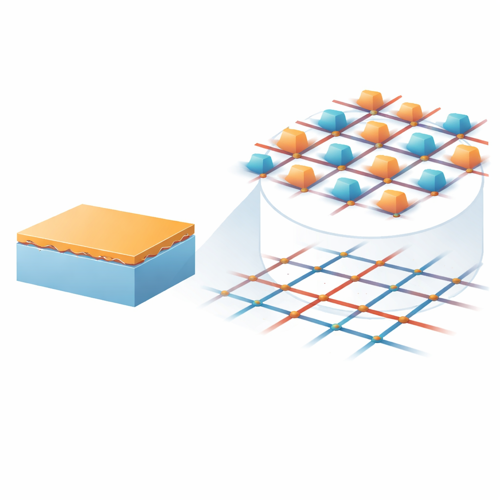
Shaping electricity with crystal imperfections
Most previous research on such exotic patterns—vortices, skyrmions, and other swirling charge textures—has focused on ferroelectrics, materials that keep a built-in electric polarization. Antiferroelectrics are their close cousins, but their internal dipoles cancel out, leaving no net polarization unless a strong electric field is applied. That very cancellation makes them attractive for high-energy capacitors and cooling devices, yet it also makes it harder to twist and rotate their tiny electric dipoles into complex shapes. The authors asked whether they could sidestep this difficulty by using something crystals naturally provide in abundance: dislocations, one-dimensional line defects that relieve strain where a film meets a mismatched substrate.
Building an ordered lattice from mismatch
The team grew ultrathin films—only about 5 nanometers thick—of the classic antiferroelectric compound lead zirconate (PbZrO3) on potassium tantalate (KTaO3) crystals. Because the two materials have slightly different atomic spacings, the film and substrate cannot fit together perfectly. High-resolution electron microscopy revealed that the interface responds by forming a dense, two-dimensional grid of dislocations running in perpendicular directions. Geometric strain mapping showed that these dislocations create a periodic landscape of compressed and stretched regions, with extremely steep strain gradients near each dislocation core that extend only a few nanometers into the film.
Electric patterns that converge and diverge
To see how this structural grid affects the film’s electric behavior, the researchers mapped the tiny displacements of lead atoms, which act as fingerprints of local polarization. They found that polarization vectors converge toward the dislocation cores and diverge in the spaces between them, forming an ordered pattern across the film. In three dimensions, each core hosts a center-converging “antihedgehog” domain, while the surrounding regions form complementary divergent structures. Together, these units tile space in a checkerboard-like lattice of alternating convergent and divergent polar textures. Plan-view images and advanced phase-contrast techniques confirmed that this pattern is not a local accident but an extended, highly regular topological array tied directly to the dislocation network.
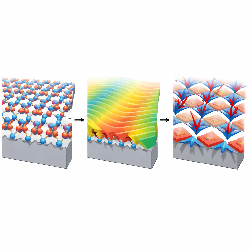
How strain gradients drive hidden order
To understand the mechanism behind this arrangement, the authors used phase-field simulations that combine elasticity, electrostatics, and the so-called flexoelectric effect, in which a strain gradient can induce polarization. The simulations reproduced the checkerboard of converging and diverging polar centers, with the convergent ones pinned to the dislocation lines. Analysis showed that two ingredients cooperate: conventional electrostriction, where strain favors certain polar orientations, and very strong, localized flexoelectric fields generated by the steep strain gradients near the dislocations. These fields can reach tens of megavolts per centimeter and are strong enough to flip the local polarization direction and stabilize the antihedgehog lattice. Chemical mapping ruled out changes in composition, indicating that the effect is purely mechanical–electrical rather than driven by impurities.
New ways to design smart, responsive materials
The antihedgehog lattice does more than just look beautiful under the microscope. Simulations reveal pockets of negative dielectric permittivity at both converging and diverging cores—a form of local negative capacitance that could help reduce power consumption in electronic switches. Experiments also show that films hosting this lattice have enhanced electromechanical response compared with thicker films where the dislocation influence has faded. Because dislocations are nearly universal in crystalline materials, the study suggests a general strategy: use built-in structural defects as a design tool to sculpt polar patterns across many compounds, not only ferroelectrics but also antiferroelectrics and other quantum materials. In simple terms, the work shows how to turn unavoidable imperfections into a precise “wiring diagram” for nanoscale electric textures, pointing toward a new generation of devices that are engineered from their topology up.
Citation: Jiang, RJ., Zhu, MX., Liu, SZ. et al. Strong interplay between polar and structural topologies. Nat Commun 17, 3882 (2026). https://doi.org/10.1038/s41467-026-70515-y
Keywords: antiferroelectric topological domains, polarization textures, dislocation engineering, flexoelectric strain gradients, nanoelectronic materials