Clear Sky Science · en
Towards universal multi-dimensional parallelization communications by direct diverse fiber/3D/2D chip hybrid integration
Why packing more data into light matters
Whenever you stream a movie, join a video call, or back up files to the cloud, your information races through hair-thin glass fibers. These fibers are reaching their limits, yet our hunger for data keeps growing. This article reports a new way to radically increase how much information can pass through a single connection by combining different kinds of optical fibers with tiny three‑dimensional and two‑dimensional chips. The result is a compact platform that can juggle hundreds of data channels in parallel, pointing toward the next generation of high‑capacity internet backbones and data centers.
Using space inside a fiber as extra lanes
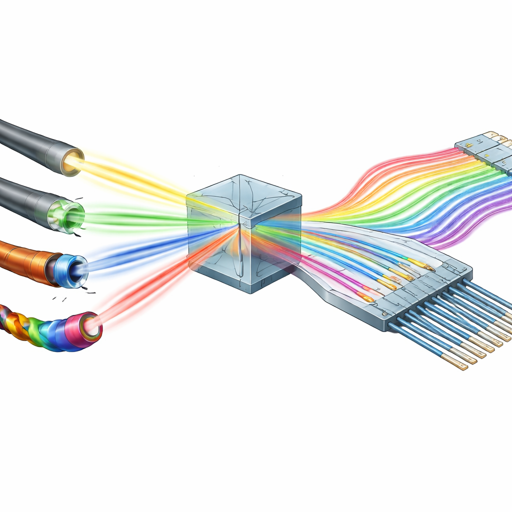
Traditional fiber links send information by changing the brightness, color, or polarization of light in a single pathway. Space‑division multiplexing instead treats the cross‑section of a fiber like a multi‑lane highway, using different cores or patterns of light as parallel channels. Several specialized fibers have been developed for this: few‑mode fibers that support a small set of light patterns, multi‑core fibers with many tiny cores bundled together, and orbital angular momentum fibers that guide light in corkscrew‑shaped paths. Each fiber type shines in certain applications, but no single one is likely to dominate. In real networks, all of them will need to coexist, and they must also talk efficiently to on‑chip waveguides that move light over millimeter or centimeter distances inside photonic circuits.
Bridging mismatched pieces with 3D and 2D chips
A major headache is that these fibers and chips have very different shapes and sizes of light fields, making direct low‑loss connections difficult. The authors tackle this by building a “bridge” chip in glass using femtosecond‑laser writing, a method that can draw three‑dimensional waveguides inside a block of silica. This 3D chip takes light coming from diverse fibers and gradually reshapes and reroutes it so that each spatial channel emerges as a neat single‑mode output. At the same time, the team shrinks the light spots enough to match the tiny silicon waveguides on a second, flat 2D chip. Careful design of curved paths, splitters, and tapered structures keeps loss and crosstalk low, allowing complex mode conversions between multi‑core, few‑mode, orbital‑angular‑momentum, and standard single‑mode fibers, as well as into on‑chip multimode waveguides.
A tiny optical hub that manages hundreds of channels
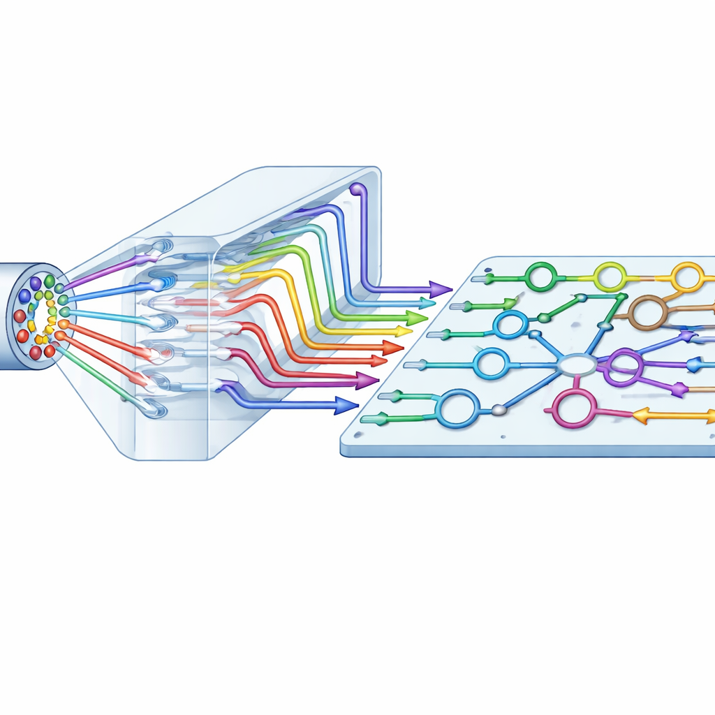
Once the spatial channels reach the silicon chip, they can be manipulated much like signals on an electronic circuit board—but in the optical domain. The authors integrate a large number of building blocks, including interferometer‑based attenuators and arrays of microscopic ring resonators. The interferometers can finely balance the power in each spatial path, while the ring resonators select or redirect specific colors of light within those paths. By designing the rings with a wide spacing between resonances, the chip can handle 36 closely spaced wavelengths per spatial channel. Eight spatial channels times 36 wavelengths yields 288 distinct optical channels that can be dynamically dropped, added, or equalized within a footprint just a few centimeters in size.
Demonstrating high‑speed data over many lanes
To prove that this intricate system works in practice, the team built a full fiber–chip–fiber communication link. They generated 36 laser wavelengths carrying advanced 16‑level encoded signals and split them into eight spatial paths using multi‑core and few‑mode fibers. These signals passed through the 3D glass chip, into the 2D silicon manager, and back out through fibers to a coherent receiver, just as they might in a real network node. Across all 288 channels, the measured error rates stayed below the threshold where standard digital error correction can clean up mistakes. Overall, the setup achieved about 30 terabits per second of data throughput—tens of thousands of high‑definition video streams’ worth of information—through a single integrated platform.
What this means for future networks
In everyday terms, this work shows how to turn a single optical link into a highly organized multi‑lane superhighway for data by combining different fibers with 3D and 2D photonic chips. Although the demonstrated capacity is still below record‑breaking laboratory systems that rely on bulky optics, the hybrid approach is compact, scalable, and compatible with chip‑making methods. The authors argue that, as these components mature and more spatial channels and wavelengths are added, similar architectures could eventually reach petabit‑per‑second capacities. That would give network designers a practical path to keep pace with exploding data demands without endlessly laying new fibers.
Citation: Li, K., Cai, C., Yan, G. et al. Towards universal multi-dimensional parallelization communications by direct diverse fiber/3D/2D chip hybrid integration. Nat Commun 17, 3771 (2026). https://doi.org/10.1038/s41467-026-70455-7
Keywords: optical communication, space-division multiplexing, silicon photonics, multi-core fiber, photonic integration