Clear Sky Science · en
Atomically sharp heteroepitaxial Hf2C edge contacts enabling barrier-free carrier injection in 2D HfSe2 semiconducting channels
Smaller, Faster Electronics Without the Usual Roadblocks
As our phones, laptops, and data centers keep shrinking and speeding up, today’s silicon-based electronics are nearing physical limits. A promising way forward uses ultra-thin “sheet-like” semiconductors only a few atoms thick. But there is a stubborn obstacle: getting electricity in and out of these sheets efficiently. This paper shows how to build an exceptionally clean, sharp connection between a metal and a two-dimensional semiconductor, allowing electric charges to flow in almost as if there were no barrier at all—an advance that could help extend computing performance well beyond current silicon technology.
Why Ultra-Thin Materials Need Better Connections
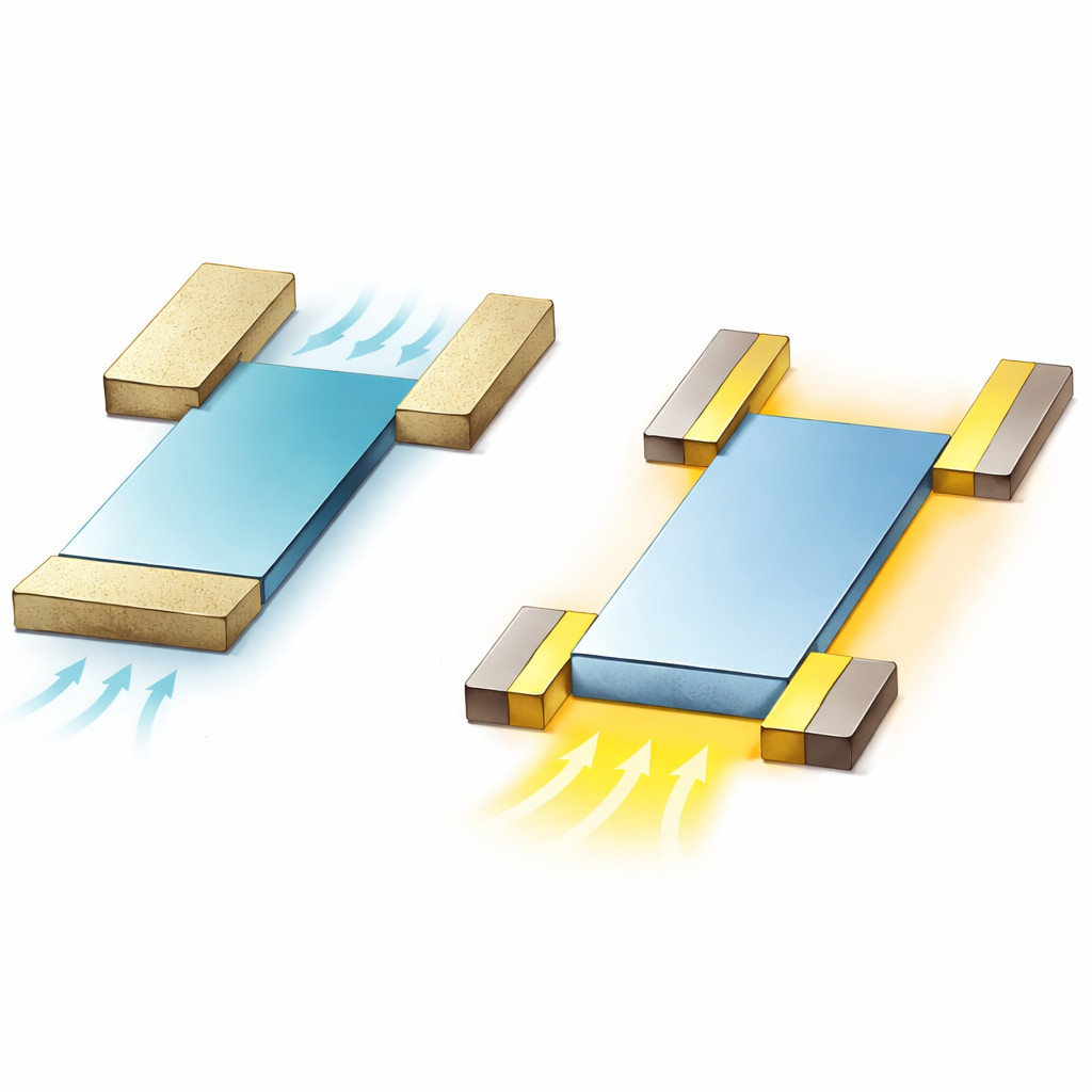
Two-dimensional semiconductors, such as HfSe2, are attractive for future transistors because their atomically thin bodies help control unwanted leakage currents and enable very dense, low-power circuits. However, their biggest weakness has been the electrical contacts that feed charges into the channel. In conventional metal contacts, the metal’s electronic “wave” leaks into the semiconductor and creates unwanted energy states in the gap where no states should exist. These so-called gap states pin the contact’s energy level, making it difficult to tailor how easily electrons can cross the junction. The result is a stubborn energy barrier and extra resistance that waste power and slow devices, even when exotic metals or clever doping schemes are used.
A New Kind of Edge Contact Grown From Within
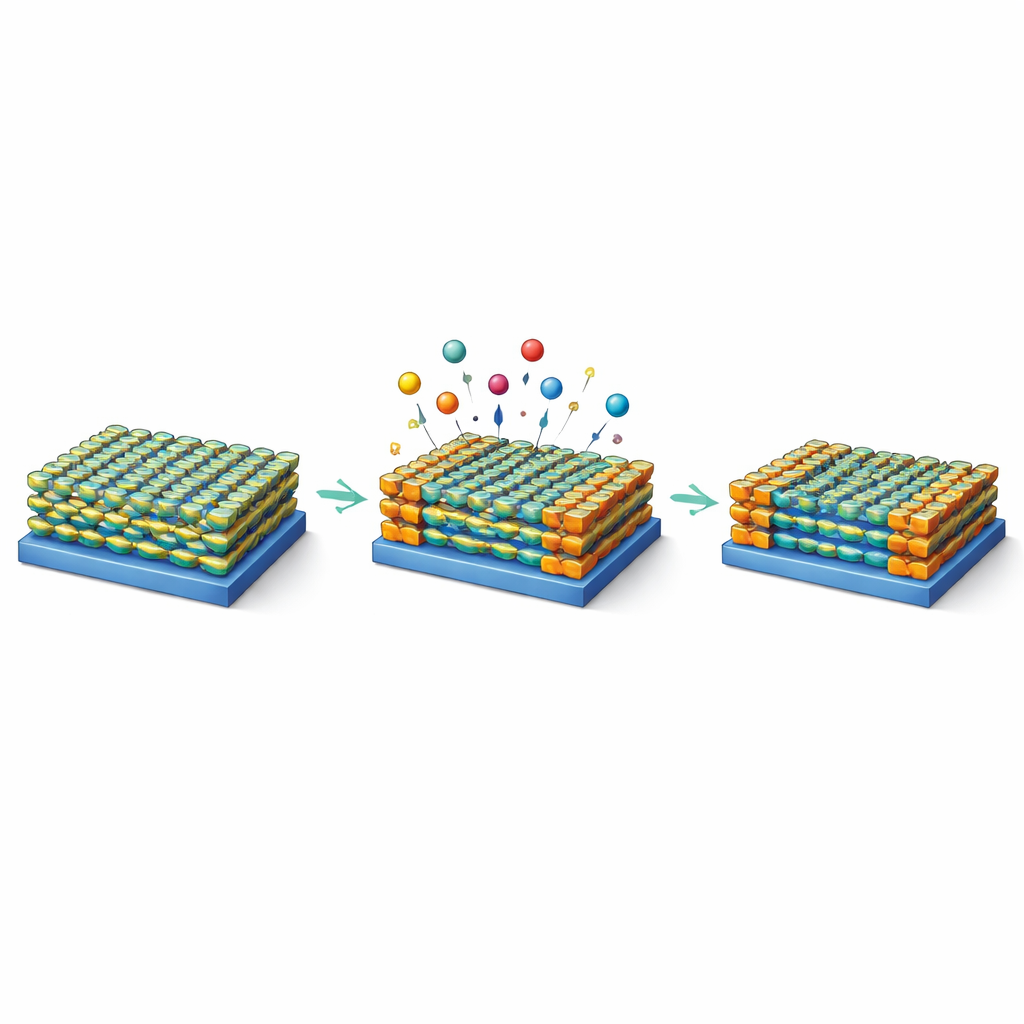
The authors tackle this problem by embedding a metallic material, Hf2C, directly into the side edges of a thicker HfSe2 sheet, forming an atomically sharp lateral junction. Instead of depositing metal on top—which tends to damage the surface—they chemically convert parts of the HfSe2 itself. Under carefully controlled conditions with methane and hydrogen gases and a copper catalyst, hydrogen atoms strip selenium from the exposed edges, while carbon-containing fragments fill in the vacant sites and bond with hafnium. As this reaction proceeds, a metallic Hf2C region grows inward from the sides, stopping where the process is timed to end. The result is a seamless, crystal-aligned interface between the metallic and semiconducting regions, defined entirely within the plane of the original sheet.
Watching Atoms Move and Electrons Flow
To understand and verify this transformation, the team combines computer simulations with advanced microscopy. Classical and quantum-level molecular dynamics simulations track how individual atoms rearrange as selenium is removed and carbon moves in, revealing that the new metallic layers are slightly tilted relative to the original HfSe2 but remain coherently bonded. High-resolution electron microscopy confirms an abrupt boundary between Hf2C and HfSe2, with distinct lattice spacings and a sharp transition over only a few atomic rows. Crucially, scanning tunneling measurements of the local electronic structure show a clean switch from metallic behavior in Hf2C to a clear bandgap in HfSe2, with no detectable states leaking into the gap at the junction. This absence of gap states signals that the usual contact problems have been largely eliminated.
Transistors That Behave As If the Barrier Is Gone
The researchers then test how these edge-embedded contacts perform in working transistors. Devices where Hf2C forms the source and drain show linear, “ohmic” current–voltage characteristics over a wide temperature range, indicating that electrons can cross the interface without needing to jump over a significant barrier. By analyzing how the current changes with temperature, they extract an effective barrier height of only about five thousandths of an electron-volt—close to barrier-free injection—and a very low contact resistance. Compared with standard metal contacts on the same material, the new edge contacts deliver much higher on-state current and maintain performance even when the contact length is shrunk, a key requirement for future, highly scaled chips.
Bringing High-Performance Logic Beyond Silicon Closer
Finally, the team integrates these edge contacts with a thin, high-quality insulating layer of HfO2 grown directly on the same HfSe2 sheet, creating a compact transistor where both the gate insulator and the contacts are engineered at the atomic scale. These devices achieve strong switching behavior close to fundamental limits, high on/off current ratios, and excellent stability over repeated operation and temperature cycling. The demonstration shows that carefully designed edge contacts, grown through controlled chemical conversion rather than simple metal deposition, can remove one of the main roadblocks to practical two-dimensional electronics. In everyday terms, the work outlines a blueprint for wiring future atomically thin chips so efficiently that electrons barely notice the junctions at all, opening a path to smaller, faster, and more energy-efficient logic circuits.
Citation: Bhin, G., Kang, T., Jin, J.W. et al. Atomically sharp heteroepitaxial Hf2C edge contacts enabling barrier-free carrier injection in 2D HfSe2 semiconducting channels. Nat Commun 17, 3770 (2026). https://doi.org/10.1038/s41467-026-70108-9
Keywords: 2D semiconductors, edge contacts, HfSe2, low-resistance interfaces, future logic devices