Clear Sky Science · en
Graded phononic metamaterials based on scalable microfabrication and design
Shaping Sound and Vibrations on a Chip
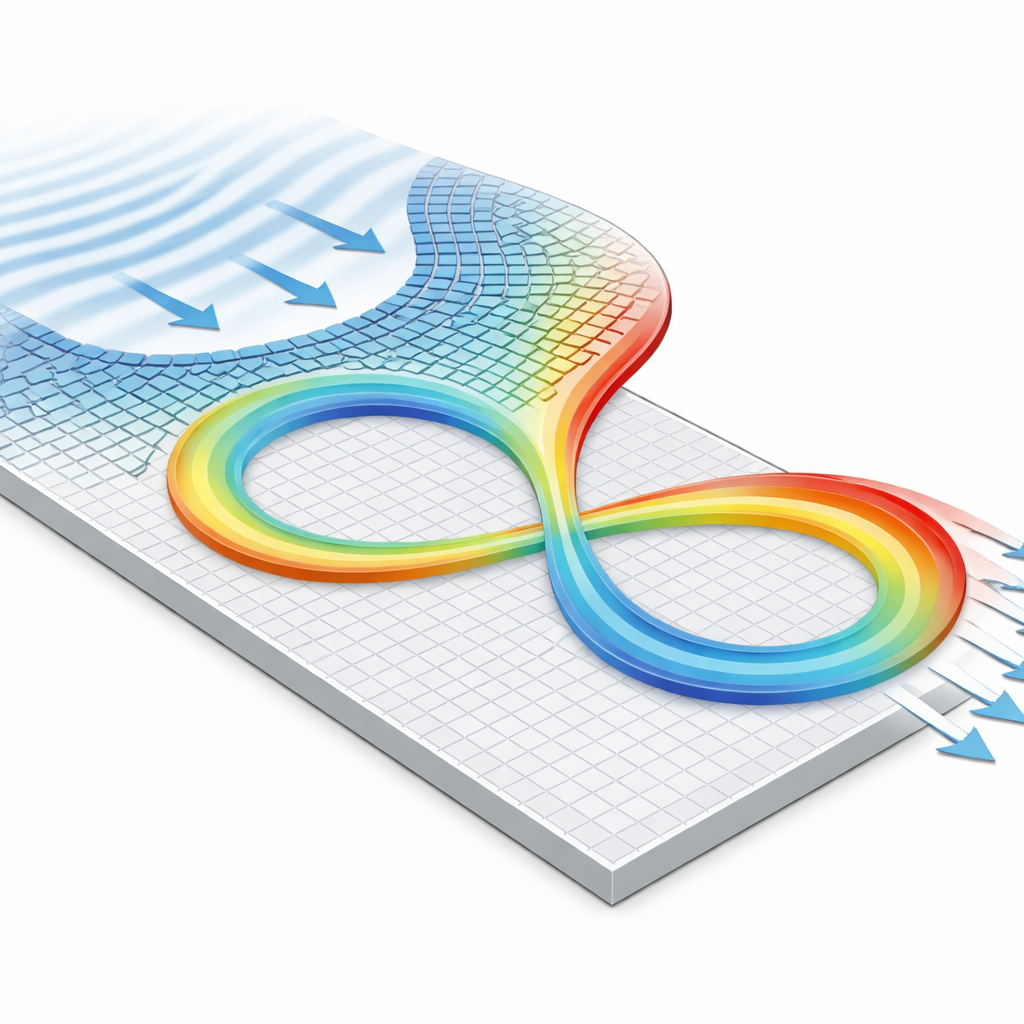
From noise-cancelling headphones to earthquake engineering, our ability to control vibrations and sound waves already shapes daily life. This research takes that control to a new level, showing how to sculpt the paths of tiny mechanical waves across a silicon chip. By designing intricate “architected” materials and fabricating them with microchip technology, the authors demonstrate that vibrations can be steered along custom tracks, such as a figure-eight loop, opening doors to ultra-compact devices for filtering signals, protecting delicate components, and harvesting energy.
Materials Built from Tiny Repeating Patterns
The work centers on “metamaterials” – materials whose unusual behavior comes not from their chemistry but from carefully engineered internal patterns. Here the patterns are made of tiny beam-like structures arranged in square blocks, or unit cells, repeated many thousands of times. These structures control mechanical waves, the same way carefully arranged glass structures can bend and focus light. Instead of leaving the pattern perfectly regular, the authors gradually change the geometry of the unit cells across the material. This smooth variation, called grading, allows waves to be guided, split, and focused along targeted paths.
Designing Wave Paths with Digital Rays
Designing such a graded material is tricky: to predict wave motion accurately, standard computer simulations must track every tiny beam, which becomes painfully slow for the hundreds of thousands of unit cells needed to behave like a true material rather than a small device. The authors sidestep this bottleneck by adapting a concept familiar from optics and seismology: ray tracing. Instead of calculating every detail of the wave field, they compute how idealized rays travel through the material, using local information about how each unit cell affects wave speed and direction. They then pose an inverse problem: adjust the unit cell shapes so that the rays follow desired curves. In this way, they design basic building blocks, or tiles, that each perform a specific steering function.
Building Complex Paths from Simple Tiles
Two key tiles are created. In the first, waves starting from a point in the center are split and steered outward to leave the tile straight through each edge. In the second, waves entering as a broad front from one side are smoothly redirected to exit through an adjacent side, effectively turning the wave by ninety degrees. By ensuring that the unit cell geometry along tile boundaries matches, these tiles can be assembled like puzzle pieces without disturbing the wave flow. Combining just a few tiles, the authors design large layouts that guide waves along intricate tracks, including a striking figure-eight loop and a cross-shaped path, each involving tens of thousands of unit cells but designed with modest computational effort.
From Silicon Wafer to Guided Waves
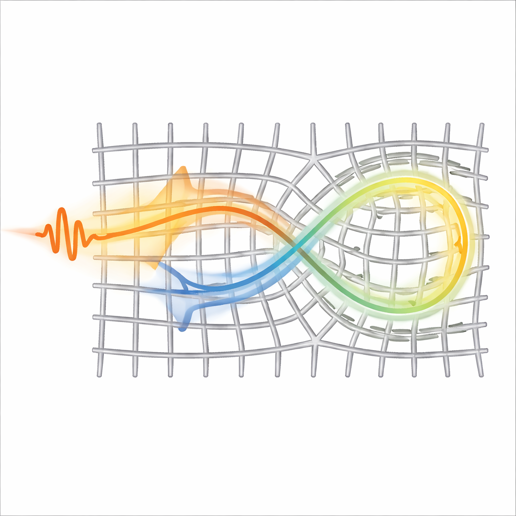
To prove these designs work in the real world, the team turns to methods used in microchip manufacturing. They sculpt the graded beam patterns into the thin top layer of standard silicon-on-insulator wafers using photolithography and deep etching. Removing the underlying sacrificial layer leaves a delicate, free-standing film of patterned silicon, stretched like a drumhead across an entire wafer region several centimeters wide. A pulsed infrared laser heats a thin metal coating on the film to trigger tiny mechanical pulses, while a sensitive optical interferometer measures the resulting motions with sub-nanometer precision at many points across the surface.
Watching Waves Obey the Design
Measurements along carefully chosen lines across the structure reveal the waves doing exactly what the design intended. A pulse launched at a single point travels along the figure-eight route, circling around and returning to the starting location. Computer simulations that fully resolve the beams mirror the experimental results, confirming that the faster ray-based design method captures the essential physics. Notably, although the structure was designed for a particular frequency, guided behavior persists across a broad band of frequencies, thanks to similarities in how the unit cells influence waves over that range.
New Ways to Control Vibrations on a Chip
The study shows that it is now possible to both design and mass-produce complex wave-guiding materials directly on silicon wafers, achieving millions of carefully arranged microstructures. For a non-specialist, the key message is that vibrations can be sculpted almost as flexibly as light in optical fibers and lenses, but now within the tiny footprint of a chip. This combination of scalable design and fabrication promises new on-chip tools for isolating sensitive components from vibration, processing mechanical signals, and harvesting otherwise wasted vibrational energy, all by programming how waves flow through an architected material.
Citation: Dorn, C., Kannan, V., Drechsler, U. et al. Graded phononic metamaterials based on scalable microfabrication and design. Nat Commun 17, 3192 (2026). https://doi.org/10.1038/s41467-026-69888-x
Keywords: phononic metamaterials, wave guiding, microfabrication, silicon wafers, mechanical waves