Clear Sky Science · en
Wafer-scale manufacturing of ultra-broadband, high-power erbium-doped integrated lasers
Tiny Chips, Big Light
Lasers are the unseen workhorses of modern technology, quietly enabling high-speed internet, precision sensing, navigation, and even medical imaging. But the very best lasers for stability and low noise have typically lived inside bulky, delicate fiber setups that are hard to mass-produce. This paper shows how researchers have brought that fiber‑class performance onto tiny silicon chips, using a process that fits into standard semiconductor factories and could make ultra-stable lasers as easy to produce as computer processors.
Why Shrinking Fiber Lasers Matters
For decades, erbium‑doped fiber lasers have set the gold standard for exceptionally pure and stable light, crucial for tasks like long-distance fiber sensing, gyroscopes, free‑space communication links, and optical clocks. Their secret lies in erbium ions, which act as a quiet, steady light amplifier with low noise and strong temperature stability. The catch is that these lasers are long coils of glass fiber assembled with great care—excellent in a lab, but awkward and expensive for widespread industrial use. Putting the same kind of light source onto a flat chip promises smaller size, lower cost, and easier integration with other photonic and electronic components, but earlier attempts have either fallen short in performance or been difficult to manufacture at scale.
Making High-Performance Lasers at Wafer Scale
The authors solve a key manufacturing bottleneck by redesigning the light‑guiding structures on the chip. Instead of using thick waveguides that require very high‑energy ion beams to implant erbium, they use much thinner silicon nitride (Si3N4) waveguides only 200 nanometers tall. This simple geometric change cuts the required implantation energy to below 500 kiloelectronvolts, which means standard 300‑millimeter industrial ion implanters—already common in semiconductor fabs—can be used. Starting from ultra‑low‑loss silicon nitride circuits on full wafers, they selectively implant erbium only where gain is needed, add glass cladding, and integrate tiny metal heaters for fine tuning. The result is a wafer full of identical, compact laser chips (each about 0.4 × 1.0 cm) produced with high throughput and without the waveguide damage that plagued earlier high‑energy approaches. 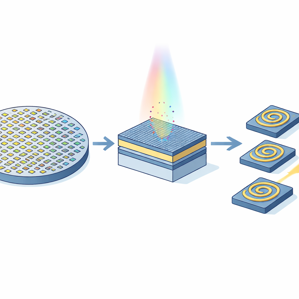
How the Chip Laser Works
Inside each chip, the laser is built as a carefully engineered optical loop. A long spiral section of erbium‑doped waveguide provides the gain, while two slightly different ring resonators act together as a “Vernier” filter that picks out one narrow color of light at a time. Adjustable loop‑shaped mirrors define the laser cavity and let engineers control how much light is fed back or sent out as useful output. The chip is pumped by a 1480‑nanometer laser—either coupled directly at the edge of the chip or delivered remotely through fiber—exciting the erbium ions so they can amplify light around the telecom C and L bands (roughly 1530–1620 nm). Micro‑heaters change the local temperature slightly, shifting the resonances of the rings and mirrors so the team can dial the lasing wavelength across a broad range while keeping the output in a single, clean spectral line. 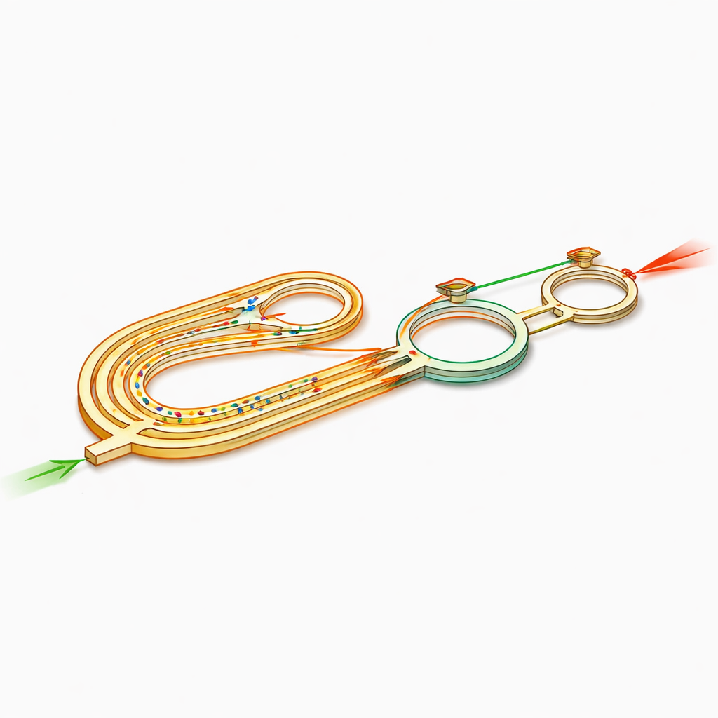
Power, Purity, and Stability
Despite their small footprint, these chip lasers deliver performance that rivals or surpasses many commercial systems. They can be tuned over 91 nanometers across the C and L bands, with fiber‑coupled output powers up to 47.6 milliwatts and a very narrow intrinsic linewidth of just 78.5 hertz—a measure of spectral purity normally associated with much larger instruments. The devices also show very low intensity and frequency noise, comparable to or better than state‑of‑the‑art fiber lasers. Because erbium’s internal energy levels are largely shielded from vibrations and heat, the lasers keep working up to 125 °C with only modest power changes, and their frequency drifts by less than 15 megahertz over six hours. Tests with deliberate back‑reflections show that the design is remarkably tolerant of optical feedback, reducing the need for bulky isolators.
What This Means for Future Technologies
To a non‑specialist, the central message is that the authors have turned a lab‑grade, delicate kind of laser into something that can be stamped out on wafers like computer chips, without sacrificing performance. By combining a foundry‑friendly silicon nitride platform with carefully engineered erbium implantation and smart cavity design, they demonstrate bright, tunable, and extremely stable lasers that can operate in harsh environments and be produced at scale. This opens the door to affordable, high‑coherence light sources for precision sensing, LiDAR, advanced communications, and many other applications where having a “perfect” laser on a chip could be transformative.
Citation: Ji, X., Yang, X., Liu, Y. et al. Wafer-scale manufacturing of ultra-broadband, high-power erbium-doped integrated lasers. Nat Commun 17, 3722 (2026). https://doi.org/10.1038/s41467-026-69787-1
Keywords: integrated lasers, silicon nitride photonics, erbium-doped devices, wafer-scale fabrication, telecom-band light sources