Clear Sky Science · en
van der Waals dielectrics for threshold engineering in two-dimensional field effect transistors
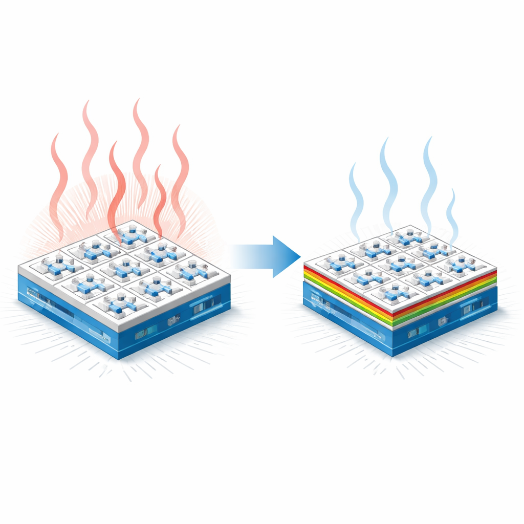
Why tiny switches matter for our power bills
Every digital device you use, from smartphones to data centers, relies on billions of microscopic switches called transistors. As engineers push these switches to become ever smaller and faster, one stubborn problem keeps growing: wasted power that turns into heat. This paper explores a new way to tame that waste in cutting-edge, atomically thin transistors by giving their “on–off knob” a precise and reprogrammable setting, potentially leading to cooler, more efficient electronics.
From promising materials to a power problem
In recent years, ultra-thin materials only a few atoms thick—known as two-dimensional semiconductors—have emerged as candidates to take over where silicon struggles. They can be made over large areas and stacked in three dimensions, promising dense, advanced chips. But when engineers try to plug these materials into the standard logic scheme used in all computers (CMOS), they run into an issue: the transistors often turn on too easily. Their threshold voltage—the point where a device clearly switches from “off” to “on”—tends to be misplaced, so even “off” transistors leak current. That background trickle wastes power continuously, especially damaging in large integrated circuits.
Why ordinary insulators fall short
To control a transistor, you need a gate electrode separated from the channel by an insulating layer. In conventional silicon chips, this layer, combined with carefully placed impurities in the silicon, sets the switching point very precisely. For two-dimensional materials, common insulators such as silicon dioxide and other oxides bring unwanted side effects: trapped charges and stray molecules at the interface push the device toward a leaky, turned-on state. Even clever tricks like encapsulating the channel with ultra-clean layers or using crystalline oxides generally improve switching sharpness but do not reliably fix the threshold to the right value for low-power CMOS logic.
A new family of “smart” insulating layers
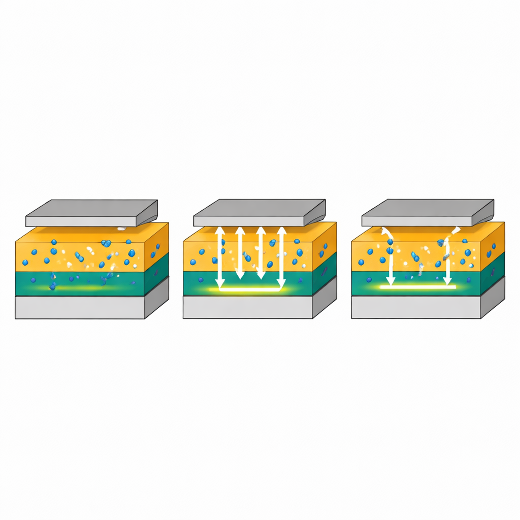
The authors turn to a different class of materials: van der Waals dielectrics, which stack like sheets of paper and form exceptionally clean interfaces with two-dimensional semiconductors. They systematically examine several candidates and identify a standout family called bimetallic thiophosphates, including a compound named LiInP2S6 (LIPS). When this material is placed above a monolayer of MoS2 (an n-type transistor) or a bilayer of WSe2 (a p-type transistor), it does more than merely insulate. Ions inside the layer—especially lithium—can drift slightly when an electric field is applied, then stay put when the field is removed. This gentle rearrangement of charge acts like a built-in, adjustable knob for the transistor’s threshold voltage, without permanently altering the semiconductor itself.
How movable ions become a memory for the switch point
By carefully sweeping the voltage on the top gate, the researchers observe a characteristic hysteresis: the transistor’s response depends on the recent history of the applied bias. Through detailed tests that vary the sweep range, speed, and temperature, they show that this behavior is best explained by slow ion migration rather than fast ferroelectric flipping. At higher temperatures or slower sweeps, the shifts become larger, consistent with ions taking time to drift and settle. Once the ions redistribute, the threshold voltage of the transistor’s back gate can be shifted in a controlled, nearly stepwise fashion. Importantly, these programmed settings remain stable over many seconds to hours, and even after up to a million programming cycles, indicating that the dielectric remains robust.
Turning better switches into better logic
With this ion-tunable dielectric in place, the team builds simple logic units called CMOS inverters from MoS2 and WSe2 devices and then programs their thresholds across different levels. They find that raising the magnitude of these thresholds—making it harder for a transistor to turn on when it should be off—can cut the static power of an inverter by nearly three orders of magnitude, down to the picowatt range, while still preserving fast switching when tuned within an optimal window. Using circuit simulations calibrated to their measurements, they show that this programmable threshold acts like built-in power gating: in active mode, settings are chosen for balanced speed and efficiency, while in sleep mode, thresholds are pushed to extremes to nearly eliminate leakage, all without adding extra “sleep” transistors that cost space and speed.
What this means for future low-power chips
At a lay level, the study shows how adding a thin, smart insulating layer packed with tame, movable ions can give atomically thin transistors a reliable and adjustable off-switch. Instead of permanently doping the material or redesigning the entire circuit, engineers can now program and reprogram the point at which each transistor wakes up or goes to sleep. This approach greatly reduces wasted current and heat, offers new ways to manage power on the fly, and preserves the advantages of ultra-thin semiconductors. If scaled and integrated into complex chips, such van der Waals dielectrics could help usher in a generation of electronics that are not only smaller and faster, but also dramatically more energy-efficient.
Citation: Sen, D., Ravichandran, H., Imam, S. et al. van der Waals dielectrics for threshold engineering in two-dimensional field effect transistors. Nat Commun 17, 2840 (2026). https://doi.org/10.1038/s41467-026-69089-6
Keywords: two-dimensional transistors, threshold voltage tuning, van der Waals dielectrics, low-power CMOS, ion migration