Clear Sky Science · en
Superior mechanoluminescence of ZnS:Mn/ZnO heterostructure array chip boosted by type II electron transition
Light from a Gentle Touch
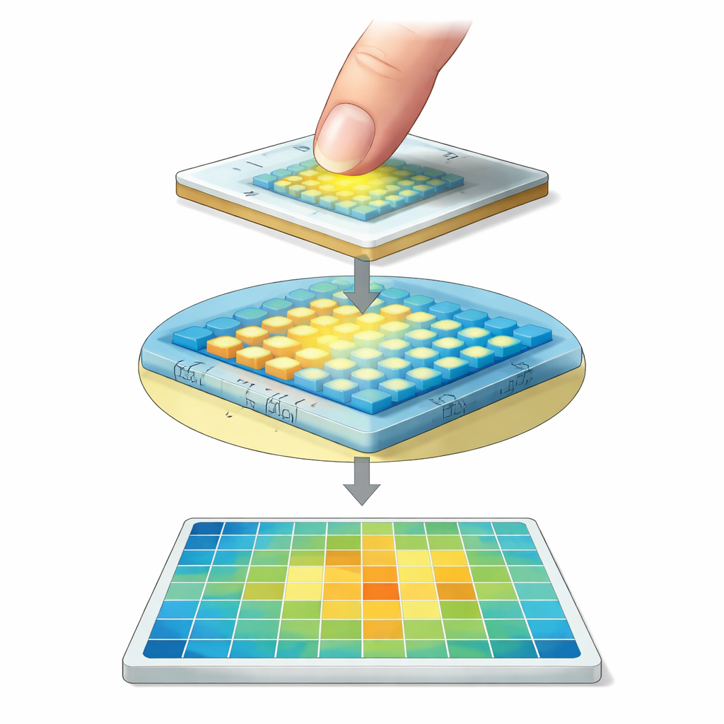
Imagine a surface that glows wherever you press it, not just with bright light but with a detailed map of how hard and where you touched. This study reports a new chip made from engineered thin films that can do exactly that, lighting up strongly even under very small forces. Such technology could underpin future electronic skin, ultra-sensitive touch sensors, and smart tools that see stress and pressure as light.
Why Making Light from Pressure Is Hard
Materials that shine when squeezed or rubbed—a phenomenon called mechanoluminescence—have been explored for years in powders mixed into rubbery plastics. These mixtures can show where stress occurs, but they behave like packed sand: many tiny grains pressing on each other in complicated ways. That complexity makes it difficult to understand how the light is really produced and limits how precisely stress can be measured. Worse, most existing systems need relatively large forces before they start to glow, which is a problem if you want to sense delicate touches, weak pulses, or small pressure variations.
Building a Light-Sensitive Chip, Not a Powder
To move beyond powders, the researchers fabricated a thin, integrated chip using standard semiconductor processing—the same kind of technology used for making computer chips. They stacked a film of zinc sulfide containing manganese (ZnS:Mn), a classic light-emitting material, on top of a zinc oxide (ZnO) layer, and carefully controlled where each material remained during a heat treatment in sulfur. This produced a regular grid of tiny square "pixels," each a well-defined junction between the two materials. Under ultraviolet light the squares glow yellow, confirming that each pixel is a controlled light-emitting region rather than a random cluster of grains. Because the pixel size can be tuned from nanometers to millimeters, the chip can, in principle, be tailored for low- or high-resolution stress imaging.
Unlocking Hidden Electrons for Brighter Glow
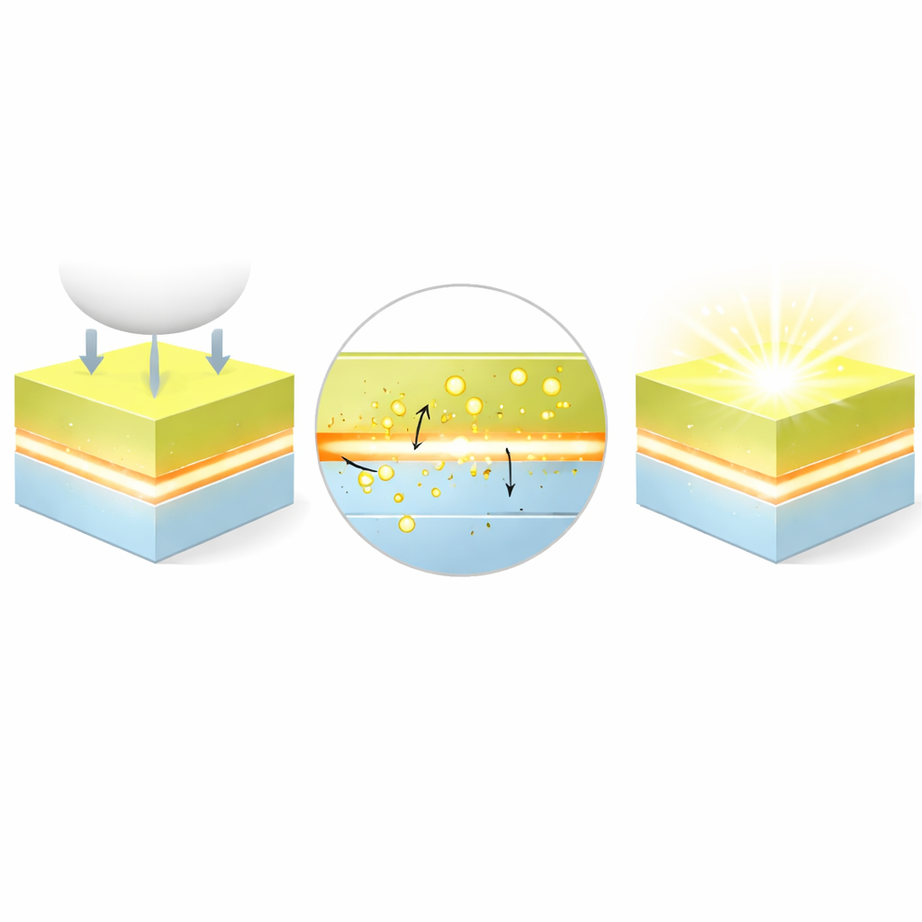
The real innovation lies in how this layered structure rearranges the energy landscape for electrons. In most earlier designs, light under pressure comes from a modest number of electrons that are either shaken loose from defects inside the material or transferred across a rubbing interface. Here, the team engineers the energy bands so that the lower-energy electrons in the deeper "valence" region of ZnS:Mn can jump directly into the higher "conduction" region of ZnO when the material is pressed. This so‑called type II transition effectively taps into a vast reservoir of previously unused electrons. Experiments show that the resulting chip emits about four times more light than similar films without the special junction and begins glowing at an extremely low force of only 0.05 newtons—roughly the weight of a small paperclip.
Seeing Force as Both Light and Electricity
Because the device is built like a true electronic component, the authors could monitor both light and electrical signals at the same time. When the ZnS:Mn/ZnO chip is pressed, brief pulses of electric current appear, and their size grows with the applied force. Conventional films of ZnS or ZnO alone do not show such current spikes under the same conditions. This indicates that pressing the heterostructure really does create extra mobile charges that flow through the more conductive ZnO layer, while their counterparts remain in the ZnS:Mn layer and help produce light. In testing, the chip behaved like a pixelated pressure camera: as a stylus scratched across it or wrote patterns, a simple imaging sensor could record glowing tracks and even estimate how hard each stroke was based on brightness.
From Glowing Chips to Electronic Skin
The study concludes that smart stacking of materials to promote type II electron transitions can radically boost the efficiency and sensitivity of pressure-induced light. By turning a familiar light-emitting powder into a clean, wafer-scale array of pixels with almost no force threshold, the authors point toward a new generation of thin, passive chips that convert touch directly into optical and electrical signals. For non-specialists, this means that future robotic hands, medical sensors, and scientific tools could literally see and measure force patterns in real time, opening the door to electronic skins and instruments that are both more sensitive and easier to integrate than today’s electronic pressure sensors.
Citation: Fan, J., Wang, Y., Zhong, A. et al. Superior mechanoluminescence of ZnS:Mn/ZnO heterostructure array chip boosted by type II electron transition. Microsyst Nanoeng 12, 143 (2026). https://doi.org/10.1038/s41378-026-01284-3
Keywords: mechanoluminescence, stress sensing, heterostructure, electronic skin, ZnS ZnO films