Clear Sky Science · en
Anchor-induced localized stress evolution and deformation prediction in SOI MEMS structures
Why tiny supports can warp tiny machines
From smartphones to car airbags, countless devices rely on microscopic machines etched into silicon chips. These microelectromechanical systems, or MEMS, often use thin silicon beams that hang over a gap, anchored only at their ends. Even slight unwanted bending in these suspended parts can blur a camera, throw off a sensor, or distort a beam of light. This study uncovers a hidden source of that bending and offers a way to predict and greatly reduce it, helping future MEMS work more accurately and reliably.
Small chips, big stress problems
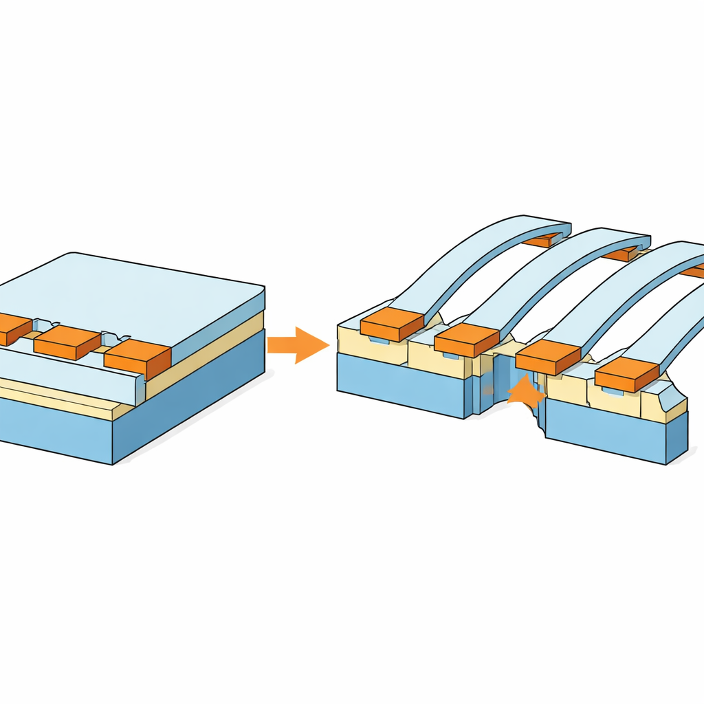
Many high‑performance MEMS are built on silicon‑on‑insulator (SOI) wafers, which stack a thin "device" layer of silicon on top of an insulating oxide layer and a thick silicon base. This architecture is prized for its mechanical stability and is used in accelerometers, gyroscopes, pressure sensors, and tunable optical components. Yet engineers have long observed that, once freed from the wafer, suspended beams and plates often curve or buckle upward by hundreds of nanometers. That may sound tiny, but for optical devices working with light whose wavelength is similar in size, even a fraction of that motion can degrade performance or cause outright failure. Until now, this deformation was usually blamed on vague “intrinsic stress” in the thin silicon itself.
Anchors as hidden troublemakers
The authors show that the main culprit is not the silicon sheet but the anchors that tie it to the buried oxide. During high‑temperature processing of an SOI wafer, silicon and oxide expand and contract differently as they heat and cool. This mismatch leaves the oxide layer squeezed in compression and the silicon layer stretched in tension. As long as everything remains bonded and unetched, these stresses are locked in and mostly harmless. Problems arise when the oxide is selectively removed to release MEMS beams: small regions of oxide remain as anchors, still under heavy compression. These anchors want to expand sideways, and when they do, they push on the bottom of the silicon beams, transferring stress into them and forcing them to bend.
How local pushing becomes global bending
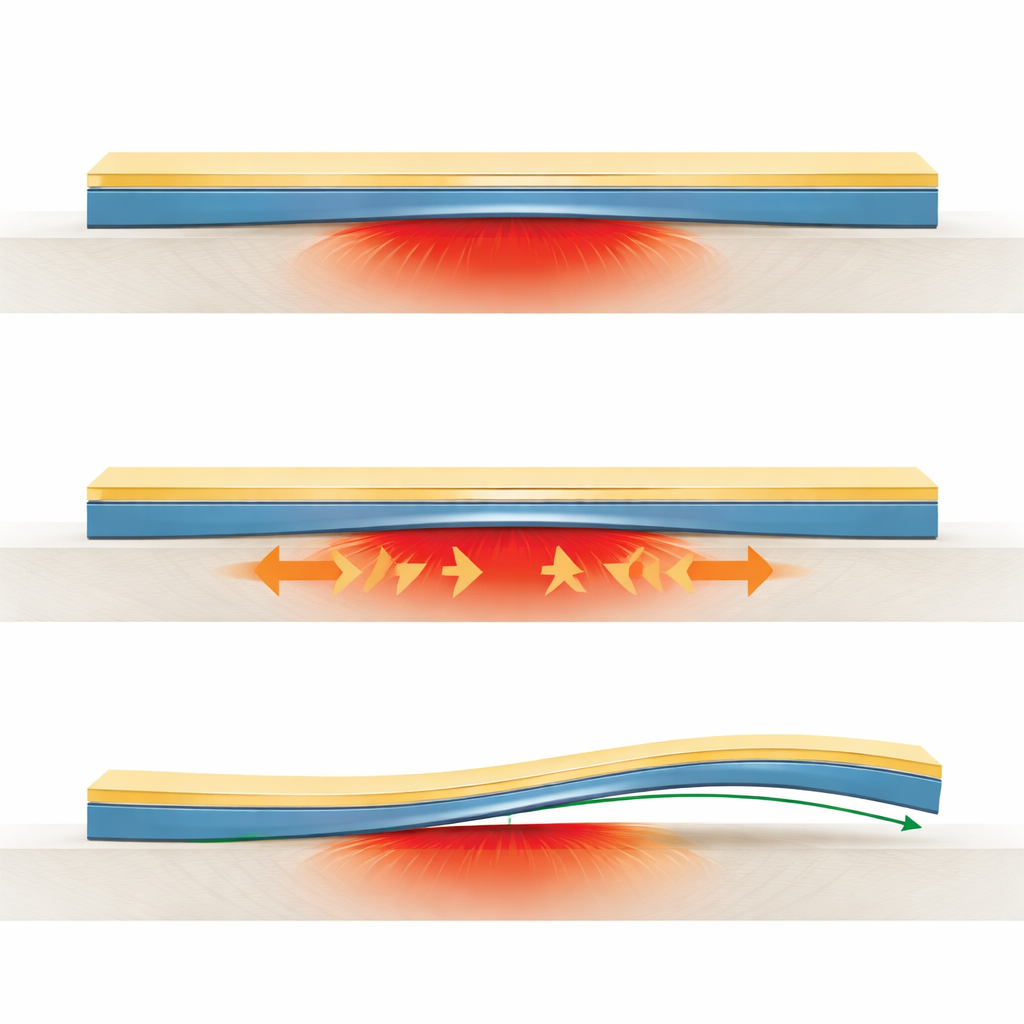
To turn this picture into a design tool, the team develops a simple mechanical model. They treat the stressed region at each anchor as an effective thin layer at the bottom of the beam that pulls it into compression and creates a localized bending moment. This local bending zone extends only a short characteristic distance along the beam before the rest of the beam behaves more like a rigid lever that simply rotates. With this idea, they derive compact formulas for the maximum deflection of both cantilever beams (fixed at one end) and double‑clamped beams (fixed at both ends). Surprisingly, for cantilevers the predicted deflection grows linearly with length, not with the higher‑power scaling expected from usual textbook loading cases, and double‑clamped beams show a sharp rise in deflection as they approach a buckling‑like limit.
Seeing and measuring the hidden stress
To check whether anchors truly drive the deformation, the researchers combined computer simulations with finely detailed experiments. Using micro‑Raman spectroscopy—essentially reading tiny shifts in the color of scattered laser light—they mapped stress on the surface of suspended plates. The measurements revealed a clear switch from tensile stress over the anchor region to compressive stress in the free, suspended parts, matching the model’s picture of stress being transferred from the oxide into the silicon beam. They then measured how real microbridges and cantilevers bent after release and compared the results with their equations and finite‑element simulations. Across many sizes and shapes, the predictions and measurements agreed within about ten percent, confirming that the simple model captures the essential physics.
Designing beams that stay flat
Armed with this understanding, the team proposed a practical fix: a stress‑isolation beam placed between the anchor and the main functional structure. In this layout, the isolation beam is oriented so that it soaks up most of the anchor‑induced compression and bending, while the central device remains largely unstressed and flat. Simulations showed that the compressive stress becomes concentrated inside the isolation beam, and measurements on fabricated samples confirmed that the main beams barely moved. In one case, the initial upward deflection of a long double‑clamped beam dropped by about 93 percent, from hundreds of nanometers down to only a few dozen.
What this means for future tiny machines
By tracing unwanted bending back to compressed oxide at the anchors, this work turns a puzzling reliability issue into a predictable, controllable design parameter. Instead of treating deformation as an unpleasant surprise to be discovered after fabrication, engineers can now estimate how much a MEMS beam will curve, adjust dimensions to stay below a safe limit, or add isolation features to block stress before it reaches critical components. The same ideas can be applied to different SOI technologies and even to other thin‑film materials on oxide. As MEMS devices push toward ever tighter tolerances—for sharper sensors, flatter optical mirrors, and more stable resonators—this anchor‑focused framework offers a clear path to keeping tiny structures straight and steady.
Citation: Hui, D., Meng, X., Ding, J. et al. Anchor-induced localized stress evolution and deformation prediction in SOI MEMS structures. Microsyst Nanoeng 12, 132 (2026). https://doi.org/10.1038/s41378-026-01277-2
Keywords: MEMS deformation, silicon-on-insulator, residual stress, microcantilever beams, anchor design